MOSFET Fabrication Traveler Wafers Specification Fall 2022
Explore the detailed process of fabricating MOSFET devices on n-type wafers, including cleaning, oxidation, doping, and more. Follow step-by-step instructions for defining source and drain, doping, and diffusion to create efficient silicon substrates.

Uploaded on | 0 Views
Download Presentation

Please find below an Image/Link to download the presentation.
The content on the website is provided AS IS for your information and personal use only. It may not be sold, licensed, or shared on other websites without obtaining consent from the author. If you encounter any issues during the download, it is possible that the publisher has removed the file from their server.
You are allowed to download the files provided on this website for personal or commercial use, subject to the condition that they are used lawfully. All files are the property of their respective owners.
The content on the website is provided AS IS for your information and personal use only. It may not be sold, licensed, or shared on other websites without obtaining consent from the author.
E N D
Presentation Transcript
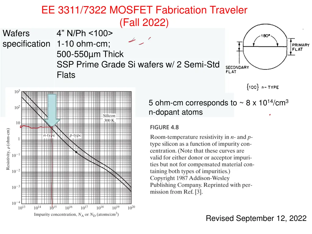
EE 3311/7322 MOSFET Fabrication Traveler (Fall 2022) Wafers specification 4 N/Ph <100> 1-10 ohm-cm; 500-550 m Thick SSP Prime Grade Si wafers w/ 2 Semi-Std Flats 5 ohm-cm corresponds to ~ 8 x 10¹⁴/cm3 n-dopant atoms Revised September 12, 2022
Step 1 - Define Source and Drain (Lab 1 and Lab2), n-type <100> wafer Notes Lab 1 Top view Side view 1-1. Clean Wafers 20 min 1:10 BOE:Water Fig. 1-1 N - D O P E D S I L I C O N S U B S T R A T E SiO2 1-2. Initial oxidation 1000 C in steam 100 sccm O2 For 5 hours 20min -target 10,000 Wet oxide Fig. 1-2 This measurement will be used for homework assignment 1-3. Measure the oxide thickness by Ellipsometer Photoresist Fig. 1-5 1-4. Dehydration bake 120 C for 20 min 1-5. Spin Resist KL 5315 3000 rpm for 30 sec Target thickness 13000 MASK 1 Fig. 1-7 1-6. Soft Bake 90 C for 1 min hotplate. 1-7. Align/Expose _4_ sec Determine the Z value for exposure: subtract 1.5 from the Z value at which mask pops Fig. 1-8 1-8. Develop in AZ726 for _45_ sec 1-9. Rinse with DI water and blow dry with nitrogen
Step 1 - Define Source and Drain (Lab 1 and Lab 2) continued Lab 2 Notes Side view Top view 1-10. Bake 120 C for 5 min 1-11. Etch field oxide in BOE full strength at 43 C for 2 min BOE 6:1 components: HF 7.13-7.3 wt%; NH4F 33.85-34.85 wt% * Fig. 1-13 1-12. Spray Rinse with DI water and blow dry with nitrogen Fig. 1-14 1-13. Inspect for complete removal of oxide Signs for complete removal of oxide: undercut along the edge of the windows (most conclusive one); White/yellow color in the windows; water beads on each die upon the wafer being taken out of the etchant; 1-14. Strip resist with acetone followed by IPA, then blow dry with nitrogen Three times 1-15. Measure Source- Drain spacing and dimensions, and take photos Sample Device 2 photo Step 1-15 (Lab 1) *http://www.kmgeci.com/products/BOE_6-1_B_408-062070_2008-12-09.pdf
Step 2 Doping of Source and Drain (Partially Offline) Lab 3 Notes Side view Top view 2-1. Pre-clean using Piranha strip mixture Sulfuric Acid :Hydrogen Peroxide (60:40) for 3 min Each day use freshly prepared Piranha strip mixture. Piranha etching makes wafer more hydrophilic (no beading) Spin-on Boron Fig. 2-3 2-2. Rinse with DI water and blow dry with Nitrogen 2-2-1 Dehydration bake on hot plate @125 C for 2min Fig. 2-4 2-3. Spin on Boron Dopant at 4000 rpm [for 30 sec] for target thickness 3000 Honeywell See manufacturer s (Honeywell) datasheet Fig. 2-5 SiO2 2-4. Pre-deposition diffusion at 1000 C (see temp profile) Fig. 2-7 2-5. Remove Spin-on Boron in HF:DI water (1:10) for 2 min @ room temperature Sign for good removal of boron: white/yellow color in the window with a slight shadow 2-6. Rinse with DI water and blow dry with Nitrogen 2-7. Drive-in diffusion at 1000 C for 80 min in steam. Target oxide thickness: 5000
Diffusion Temperature Profile of Step 2 (in previous page) I. Predeposition diffusion temperature profile ( corresponding to 2-4 in Step 2) II. Drive-in diffusion temperature profile ( corresponding to 2-7 in Step 2) 1000 0C for 80 min 25oC 25oC The temperature ramp is the wafer temperature change from the room temperature to the furnace temperature when loading or unloading the wafers to the furnace. This loading or unloading wafers step takes about 3-4 minutes.
Step 3 - Define Gate and Pre-Contacts (Lab 4 and Lab 5) Side view Top view Photoresist Lab 4 Notes Lithography for Gate Fig. 3-2 3-1. Bake 120 C for 20 min Note cross sections not to scale. 3-2. Spin Resist KL 5315 at 5000 rpm for 30 sec Target thickness ~1.1 m MASK 2 Fig. 3-4 3-3. Soft Bake 90 C for 1 min 3-4. Align/Expose _3.0_ Sec Find out the Z value for exposure before alignment. Determine the Z value for doing alignment: Subtract 2 from the Z value for exposure Fig. 3-5 3-5. Develop in AZ726 for _60_ sec 3-6. Blow dry with Nitrogen Sample Device 2 photo Step 3-5
Notes for Lab 3 Alignment: 1) Align streets and alleys for rough alignment 2) Use device 34 for fine alignment 3) Check device two and make sure the ratio between source/gate overlap and drain/gate overlap is no greater than 0.7 as well as centered
Step 3 - Define Gate and Pre-contacts (Lab 4 and Lab 5) continued Lab 5 Notes 3-7. Bake 120 C for 5 min Top view Side view 3-8. Etch field oxide in BOE full strength at 38 C for 1 and 1/2 min for whole wafer, 10 more sec for thicker parts Oxide in the gate takes longer than that in the pre-contacts to remove Fig. 3-9 3-9. Spray Rinse with DI Water and blow dry with Nitrogen Fig. 3-12 3-10. Inspect for complete oxide removal All three windows (gate and two pre-contacts) have to look clear SiO2 3-11. Strip Resist with Acetone followed by IPA, then blow dry with nitrogen Three times Fig. 3-17 3-12. Inspect and take photos 3-13. Pre-gate cleanup in piranha strip H2SO4:H202 (60:40) for 5 min Each day use freshly prepared piranha strip 3-14. Rinse with DI water for 3 min and blow dry with nitrogen 3-15. Gate oxidation at 1000 C in oxygen for 80 min and measure gate oxide thickness Target 700 900 Color chart can be used to estimate gate oxide thickness Sample Device 2 photo Step 3-14 (Lab 5)
Notes for Lab 5 Etching: If color appears in source, gate, or drain where photoresist does not protect Device 2, wafer will need additional etching to remove exposed oxide A fully etched Device 2 should all be uniformly light grey/white in color Removal of photoresist will uncover oxide not etched in BOE
Step 4 - Define Contacts (Lab 6 and Lab 7) Top view Side view Photoresist Lab 6 Notes Lithography for Contacts Fig. 4-2 4-1. Bake 120 C for 20 min 4-2. Spin Resist KL 5315 at 4500 rpm for 30 sec Target thickness 12000 MASK 3 Fig. 4-4 4-3. Soft Bake 90 C for 1 min 4-4. Align/Expose _4.0_ sec Challenging for the eyes because the entire device pattern is covered by the red pattern on mask except the two little contact windows. Fig. 4-5 4-5. Develop in AZ726 for 1 min 4-6. Rinse with DI water and blow dry with nitrogen Sample Device 2 Step 4-5 (Lab 4)
Step 4 - Define Contacts (Lab 6 and Lab 7) continued Lab 7 Notes Side view Top view 4-8. Hard bake on hot plate at 120 C for 5 min 4-9 Etch field oxide in BOE full strength at room temp for 1min 30 seconds Gate oxide does not take that much longer time to remove than previous oxides Fig. 4-9 4-10. Rinse with DI water and blow dry with nitrogen Fig. 4-12 4-11. Inspect for complete oxide removal 4-12. Strip Resist with Acetone & IPA, then blow dry with nitrogen Three times 4-14. Inspect and take photos Sample Device 2 photo Step 4-14 (Lab 4)
Step 5 Metallization (Lab 8 and Lab 9) Top view Side view Lab 8 Notes Aluminum 5-1. Deposit alloy of aluminum silicon- copper using RF Sputter (offline) Target 7000 9000 15 min AR 30sccm 400W RF Fig. 5-1 Lithography for Probe Points Fig. 5-3 5-2. Bake 120 C for 20 min (off-line) 5-3. Spin Resist KL 5315 at 5000 rpm for 30 sec Target thickness ~ 1.1 m Fig. 5-5 MASK 4 5-4. Soft Bake 90 C for 1 min Fig. 5-6 5-5. Align/Expose _3.5_ sec 5-6. Develop in AZ726 for 1 min 5-7. Rinse with DI water and blow dry with nitrogen Sample Device 2 photo Step 5-6 (Lab 5)
Top view Side view Step 5 Metallization (Lab 8 and Lab 9) continued Lab 9 Notes Fig. 5-9 5-8. Hard bake on hot plate at 120 C for 5 min 5-9. Etch aluminum in 16:1:1:2 Al etch at 30 35 C till clear plus 15 sec Phospheric acid: 73 wt%; acetic acid:1.3-5 wt%; nitric acid: 3.2 wt%; water: 18-22 wt%* Fig. 5-12 5-10. Rinse with DI water and blow dry with nitrogen 5-11. Inspect 5-12. Strip resist with acetone followed by IPA, then blow dry with nitrogen Three times 5-13. Inspect and take photos Sample Device 2 photo Step 5-13 (Lab 5) *http://sct.uab.cat/l-amb-controlat/sites/sct.uab.cat.l-amb-controlat/files/AlEtch.pdf
Step 6 Alloy and Test (Lab 10) Lab 10 Notes 6-1. Alloy at 350 C for 20 min 6-2. Test devices Wafer probe setup (Lab 10) Device 2 IV curve (Lab 6)
List of Test Structures on 3311 Chip This chip is a metal-gate, thick-oxide, PMOS process with boron diffused junctions 1-3. Wide thin-oxide devices of various L s. 4-6. Narrow thin-oxide devices of various L s. 7-9. Narrowest thin-oxide devices of various L s. 10. Short field device. 11. Longer field device. 12. Longest field device. 13. Super-tiny thin-oxide device. Probably won t work. 14. Bond pad on field oxide. 15. Larger-area metal on field oxide. 16. Metal-to-diffusion thin-oxide capacitor. 17. Diffusion capacitor. 18. Diffusion serpentine with four (Kelvin) contacts for diffusion sheet resistance. 19-20. Vertical and horizontal contact-to-diffusion alignment measurement device. 21. Metal-diffusion contact string. Use to check contact integrity. 22. Thin metal serpentine with four (Kelvin) contacts for metal sheet resistance. This device is probably too narrow to be etched without breaking the connections. 23. Metal serpentine over diffusion serpentine. Use to check metal continuity and diffusion sheet resistance. 24. Metal to diffusion alignment measurement device without gate oxide: use to automatically measurement metal to diffusion alignment. 25. Metal to diffusion alignment measurement device with gate oxide: use to automatically measurement metal to diffusion alignment, or gate oxide to diffusion alignment.
List of Test Structures on 3311 Chip, contd 26-30. Diffusion-to-diffusion spacing, going from widest on left to narrowest on right. Use to check if diffusions are touching, or to measure punch-through. 31. Metal-to-diffusion capacitor. Metal to the left; diffusion to the right. 32. Enhancement-load ratioed inverter: Bond pads, going clockwise and starting at 12 o clock: VDD; output; VSS; input; VGG. 33. Sample-and-hold gate. Bond pads, going clockwise and starting at 2 o clock: Sense transistor source or drain; sense transistor drain or source; sample gate; input. 34. Alignment cross: thin oxide to diffusion. 35. Alignment cross: contact to thin oxide. 36. Alignment cross; metal to contact. 37. A lateral grounded-base PNP transistor. The emitter is at the top, and the collector is at the bottom. The n-type substrate is the base. 38. A sixteen-stage shift-register. Bond pads, going clockwise and starting at 12 o clock: VDD, VSS Phase 2 Clock, Output, VGG, VDD, VSS, Input, Phase 1 Clock. 39. A ring oscillator with fifteen inverters and a buffer. Bond pads, going clockwise and starting at 1 o clock: VDD; output from buffer; VSS; VGG. 40. Ring oscillator with thirty-five inverters plus output buffer connected to, but not in the ring. Bond pads, going clockwise and starting at 1 o clock: VDD; output from buffer; VSS; gate to provide input for 25 inverter ring; gate to provide input for 15 inverter ring; gate to provide input for 35 inverter ring; VGG. The intermediate taps for inputs likely will not work since the input will be contending with the fixed output of the previous stage. Circuits 38, 39, and 40 may not work due to design-rule violations in the metal leads which results in many of the circuit connections being not connected. Note: many years ago we made some changes to the mask set so that circuits 38, 39 and 40 would have a better chance of working. However, we just noticed that we are still using the old mask set for EE 3311.

, n-type")
")
")
")
")

")

")
")
")

")