Explore the functionalities of multiplexers, decoders, and programmable logic devices in this detailed chapter covering topics like Three-State Buffers, Read-Only Memories (ROMs), and Complex Programmable Logic Devices (CPLDs). Understand how to implement various logic functions using these components effectively.
Please find below an Image/Link to download the presentation.
The content on the website is provided AS IS for your information and personal use only. It may not be sold, licensed, or shared on other websites without obtaining consent from the author. If you encounter any issues during the download, it is possible that the publisher has removed the file from their server.
You are allowed to download the files provided on this website for personal or commercial use, subject to the condition that they are used lawfully. All files are the property of their respective owners.
The content on the website is provided AS IS for your information and personal use only. It may not be sold, licensed, or shared on other websites without obtaining consent from the author.
E N D
Presentation Transcript
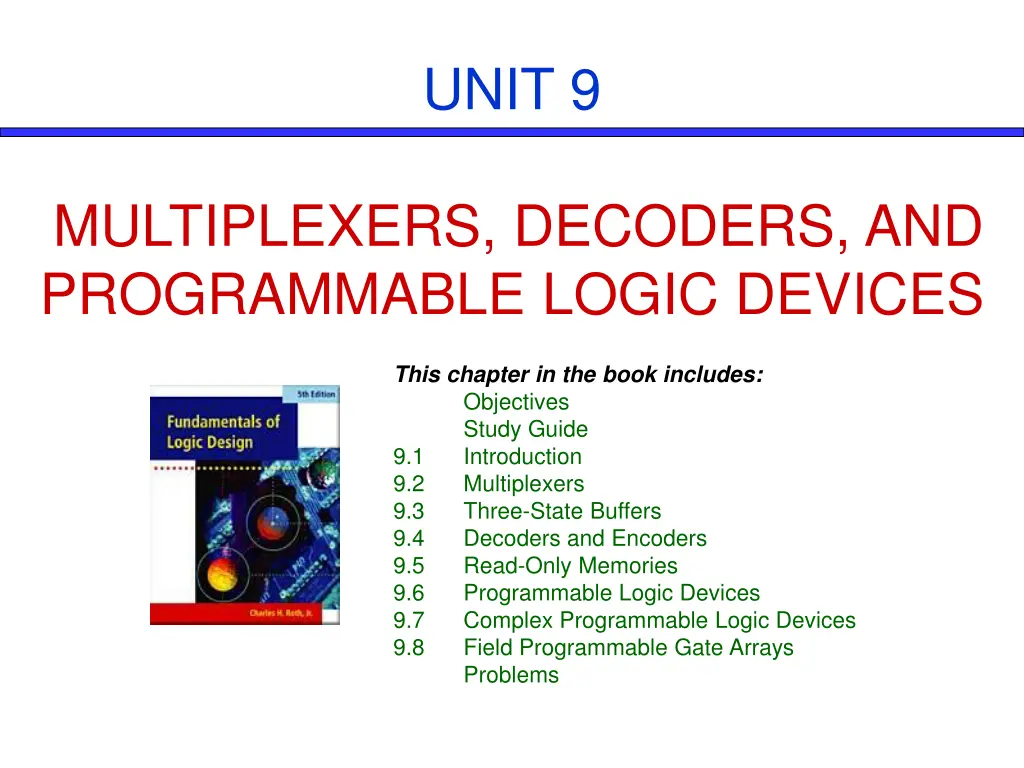
UNIT 9 MULTIPLEXERS, DECODERS, AND PROGRAMMABLE LOGIC DEVICES This chapter in the book includes: Objectives Study Guide 9.1 Introduction 9.2 Multiplexers 9.3 Three-State Buffers 9.4 Decoders and Encoders 9.5 Read-Only Memories 9.6 Programmable Logic Devices 9.7 Complex Programmable Logic Devices 9.8 Field Programmable Gate Arrays Problems
Objectives 1. Explain the function of a multiplexer and implement a multiplexer using gates. 2. Explain the operation of three-state buffers. Determine the resulting output when three-state buffers outputs are connected together. Use three-state buffers to multiplex signals onto a bus. 3. Explain the operation of a decoder and encoder and use a decoder with added gates to implement a set of logic functions. Implement a decoder or priority encoder using gates. 4. Explain the operation of a read-only memory (ROM) and use a ROM to implement a set of logic functions. 5. Explain the operation of a programmable logic array (PLA). Use a PLA to implement a set of logic functions. Given a PLA table or an internal connection diagram for a PLA, determine the logic functions realized. 6. Explain the operation of a programmable array logic device (PAL). Determine the programming pattern required to realize a set of logic function with a PAL. 7. Explain the operation of a complex programmable logic device (CPLD) and a field programmable gate array (FPGA). 8. Use Shannon s expansion theorem to decompose a switching function.
9.2 Multiplexers Multiplexer (MUX, Data Selector) 2-to-1 Multiplexer and Switch Analog Logic equation for the 2-to-1 MUX = + ' Z A I AI 0 1
9.2 Multiplexers 4-to-1 Multiplexer Logic equation for the 4-to-1 MUX = + + + ' ' ' ' Z A B I A BI AB I ABI 0 1 2 3
9.2 Multiplexers 8-to-1 Multiplexer Logic equation for the 8-to-1 MUX = + + + ' ' ' C ' ' ' ABC ' ' Z A + B C I A + B CI A + BC I A BCI 0 ' 1 2 3 + ' ' ' AB I AB CI I ABCI 4 5 6 7
9.2 Multiplexers 2n-to-1 Multiplexer Logic equation for the 2n- to - 1 MUX n 2 1 = k mk : minterm of the n control variables Ik: corresponding data input = Z m kI k 0
9.2 Multiplexers Quadruple 2-to-1 Multiplexer Used to Select Data
9.2 Multiplexers Quad Multiplexer with Bus Inputs and Output X, Y : Bus input Z : Bus output
9.3 Three-State Buffers Gate Circuit with Added Buffer The logic of the buffer input and output are the same (F = C) Buffer is used to increase driving capability
9.3 Three-State Buffers Three-State Buffer Tri-State Buffer High-impedance (Hi-Z) state The output is enabled when B = 1, disabled when B = 0
9.3 Three-State Buffers Four Kinds of Three-State Buffers B A C B A C B A C B A C 0 0 0 1 1 0 1 1 Z Z 0 1 0 0 0 1 1 0 1 1 0 1 Z Z 0 0 0 1 1 0 1 1 Z Z 1 0 0 0 0 1 1 0 1 1 1 0 Z Z (a) (c) (b) (d)
9.4 Decoders and Encoders Realization of a Multiple-Output Circuit Using a Decoder = = n , to 0 or 2 (noninvert 1 ed outputs) y m i i i = i y = i m = n , to 0 2 (inverted 1 outputs) M i i = + + ( , , , ) f a b c d m m m 1 1 2 4 = ( ' ' )' ' 4 m m m 1 2 = + + ( , , , ) f a b c d m m m 2 4 7 9 = ( ' ' )' ' 9 m m m 4 7
9.4 Decoders and Encoders 8-to-3 Priority Encoder y0 y1 y2 y3 y4 y5 y6 y7 a b c d 0 1 X X X X X X X 0 0 1 X X X X X X 0 0 0 1 X X X X X 0 0 0 0 1 X X X X 0 0 0 0 0 1 X X X 0 0 0 0 0 0 1 X X 0 0 0 0 0 0 0 1 X 0 0 0 0 0 0 0 0 1 0 0 0 0 0 1 1 1 1 0 0 0 1 1 0 0 1 1 0 0 1 0 1 0 1 0 1 0 1 1 1 1 1 1 1 1
9.5 Read-Only Memories An 8-Word x 4-Bit ROM A B C F0 F1 F2 F3 0 0 0 0 1 1 1 1 0 0 1 1 0 0 1 1 0 1 0 1 0 1 0 1 1 1 0 0 1 0 1 0 0 0 1 1 1 0 1 1 1 1 1 0 0 0 1 0 0 0 1 1 0 1 1 1 typical data stored in ROM (23 words of 4bits each) (b) Truth table for ROM (a) Block diagram
9.5 Read-Only Memories Read-Only Memory with n Inputs and m Outputs n input Variables m output Variables 00 00 00 00 00 01 10 11 100 010 101 110 110 111 101 010 011 110 000 101 typical data array stored in ROM 11 11 11 11 00 01 10 11 001 110 011 111 (2nwords of m bits each)
9.5 Read-Only Memories An 8-Word x 4-Bit ROM = = + ' ) 6 , 4 , 1 , 0 ( m ' ' F A B AC 0 = = + ) 7 , 6 , 4 , 3 , 2 ( m ' F B AC 1 = = + ' ) 6 , 2 , 1 , 0 ( m ' ' F A B BC 2 = = + ) 7 , 6 , 5 , 3 , 2 ( m 4 F AC B 3
9.5 Read-Only Memories Equivalent OR Gate for F0 = = + ' ) 6 , 4 , 1 , 0 ( m ' ' F A B AC 0
9.6 Programmable Logic Devices PLA Table for Figure 9-25 Product Term Inputs Outputs A B C F0 1 1 0 0 0 F1 0 1 1 0 0 F2 1 0 0 1 0 F3 0 0 1 0 1 = + ' ' ' F A B AC 0 0 1 - - 1 0 - 1 1 - - 0 - 0 1 A B AC B BC AC = + ' F AC B 1 = + ' ' ' F A B + BC 2 = F B AC 3
9.6 Programmable Logic Devices PLA Realization of Equations (7-23b) (p194) = + ' + + ' ' ' ' f a bd + abd ab c b c 1 = f c a bd 2 = + + ' ' f bc ab c abd 3 a b c d f1 1 1 1 1 0 0 f2 1 0 0 0 1 0 f3 0 1 1 0 0 1 0 1 1 - - - 1 1 0 0 - 1 - - 0 1 1 1 1 1 - - - - (a) PLA table
9.8 Field Programmable Gate Arrays Implementation of a Function Generator (Lookup Table, LUT) a b c d f 0 0 1 0 0 1 0 0 1 0 1 1 0 1 1 = + ' + + + ' + + ' + ' ' ' ' ' ' ' ' ' ' ' ' ' F a b c d a b cd a bc d a bcd ab c d ab cd abc d abcd
9.8 Field Programmable Gate Arrays Decomposition if switching Functions = + = + ( , , , ) ' , 0 ( , , ) , 1 ( , , ) ' f a b c d a f b c d af b c d a f af 0 1 = + + + ( , , , ) ' ' ' + ' ' f a b c d c d a b c bcd + ac + = + + ( ' a ' ' ' ) + ( c ' ' ) ' c c d b c bcd a c + d bcd = = + + + ( ' a ' ' ' ) ( ' ) ' c d b c cd a bd a f af 0 1 ( , ,..., 1 , 0 , ,..., ) f x x x x x + 1 ' 2 ( 1 i ,..., i , 0 , n ,..., = + , ) ( , ,..., 1 , 0 , ,..., ) x f x + x x x x x f x x x x x + + 1 2 1 1 1 2 1 i i i n i i i n = ' x f x f 0 i i i
9.8 Field Programmable Gate Arrays Decomposition if switching Functions = + = + ( , , , , ) ' , 0 ( , , , ) , 1 ( , , , ) ' f a b c d e a f b c d e af b c d e a f af 0 1 = + = + ( , , , , , ) ' , 0 ( G , , , , ) , 1 ( , c , d , e , ) ' G a b c d e f a b c d e f aG b c d e f a G aG 0 1 = + = + ' , 0 , 0 ( G , , , ) , 1 , 0 ( , d , e , ) ' G b c d e f bG f b G bG 0 00 01 = + = + ' , 0 , 1 ( G , , , ) , 1 , 1 ( , , , ) ' G b c d e f bG c f b G bG 1 10 11 = + + + ( , , , , , ) ' ' ' ' G a b c d e f a b G a bG ab G abG 00 01 10 11