Explore the need for multistage amplifiers, gain calculations, different types, frequency responses, voltage vs. power amplifiers, feedback principles, transistor applications, operational amplifier functionalities, and more in the field of electronics.
Please find below an Image/Link to download the presentation.
The content on the website is provided AS IS for your information and personal use only. It may not be sold, licensed, or shared on other websites without obtaining consent from the author. If you encounter any issues during the download, it is possible that the publisher has removed the file from their server.
You are allowed to download the files provided on this website for personal or commercial use, subject to the condition that they are used lawfully. All files are the property of their respective owners.
The content on the website is provided AS IS for your information and personal use only. It may not be sold, licensed, or shared on other websites without obtaining consent from the author.
E N D
Presentation Transcript
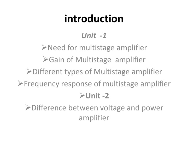
introduction Unit -1 Need for multistage amplifier Gain of Multistage amplifier Different types of Multistage amplifier Frequency response of multistage amplifier Unit -2 Difference between voltage and power amplifier
Class A, Class B, Class C, Class AB amplifier Single Ended power amplifier Collector Efficiency and distortion in class A,B,C Heat dissipation curve and importance of heat sinks Single and double Tuned voltage amplifier Unit -3 Basic principal and types of Feedback R-C coupled amplifier with emitter bypass capictor
Emitter follower and its application Transistor Amplifier Unit -4 Use of positive feedback Unit 5 Working principal of Transistor as switch Concept of multi-vibrator
Bistable multi-vibrator and application Block diagram of IC555 and its working and application Characteristics of an ideal operational amplifier IC- 741 and its pin digram Unit -6 Differential voltage gain CMMMR, PSRR, slew rate and input offset current
Multi-Stage Transistor Amplifier In practical applications, the output of a single state amplifier is usually insufficient, though it is a voltage or power amplifier. Hence they are replaced by Multi-stage transistor amplifiers. In Multi-stage amplifiers, the output of first stage is coupled to the input of next stage using a coupling device. These coupling devices can usually be a capacitor or a transformer. This process of joining two amplifier stages using a coupling device can be called as Cascading. The following figure shows a two-stage amplifier connected in cascade.
The overall gain is the product of voltage gain of individual stages. AV=AV1 AV2=V2/V1 V0/V2=V0/V1 Where AV= Overall gain, AV1= Voltage gain of 1ststage, and AV2= Voltage gain of 2ndstage. If there are n number of stages, the product of voltage gains of those n stages will be the overall gain of that multistage amplifier circuit.
Multi-stage amplifiers are used in electronic circuits for several reasons. Here are some of the primary reasons for using multi-stage amplifiers: Gain: Multi-stage amplifiers provide a higher overall voltage or power gain compared to a single-stage amplifier. By cascading multiple amplifier stages, you can achieve a much larger amplification of the input signal. This is essential when the input signal is very weak, and you need a substantial output signal. Bandwidth: Single-stage amplifiers often have limited bandwidth due to their internal capacitance and other limitations. Multi-stage amplifiers can be designed to have wider bandwidths, making them suitable for amplifying a broader range of frequencies. Impedance Matching: Multi-stage amplifiers can be used to match the impedance between different parts of a circuit. This is especially important when connecting a source with a high output impedance to a load with a low input impedance or vice versa. Each stage can be designed to provide the appropriate impedance transformation. Distortion Reduction: In some cases, a single amplifier stage may introduce distortion or nonlinearity. By using multiple stages, it's possible to mitigate the effects of distortion and nonlinear behavior in each stage, resulting in cleaner output signals. Isolation: Multi-stage amplifiers can provide isolation between different parts of a circuit. This can be beneficial in preventing interactions or interference between components or stages.
Specialized Functions: In some applications, each stage of a multi-stage amplifier can perform a specialized function, such as filtering, frequency response shaping, or equalization. This allows for a more versatile and tailored amplification process. Compensation: In cases where one amplifier stage introduces a phase shift or other undesirable effects, additional stages can be added to compensate for these effects, providing a more accurate overall amplification. Reduced Noise: Multi-stage amplifiers can help reduce the impact of noise introduced by each stage. In some cases, the noise from one stage can be partially canceled out by the following stages, resulting in a cleaner output signal. Modularity: Multi-stage amplifiers are modular and can be easily customized or expanded by adding or removing stages to meet specific requirements or adapt to different input sources. In summary, multi-stage amplifiers offer advantages in terms of gain, bandwidth, impedance matching, distortion reduction, isolation, and specialized functions. They are commonly used in various electronic applications to achieve specific performance goals and adapt to the requirements of the input and output signals.
Gain of multi stage amplifier The gain of a multi-stage amplifier is the product of the gains of its individual amplifier stages. Each stage contributes to the overall gain, and when you cascade multiple amplifier stages, you can calculate the total gain by multiplying the gains of each stage. Mathematically, if you have 'n' amplifier stages with gains represented as A1, A2, A3, ..., An, then the total gain calculated as: A total = A1 * A2 * A3 * ... * An For example, if you have a two-stage amplifier with a first stage gain (A1) of 10 and a second stage gain (A2) of 20, the total gain of the multi-stage amplifier would be: A total = 10 * 20 = 200 So, the overall gain of the two-stage amplifier is 200. It's important to note that the actual gain may also take into account factors such as the input and output impedances of the stages, and any loading effects. Therefore, while this multiplication of gains gives an idealized view of the gain, real-world considerations may affect the actual gain. Additionally, the frequency response and bandwidth of each stage can also impact the overall performance of the multi-stage amplifier.
Different Types of multistage amplifier Multistage amplifier A multistage amplifier is an electronic amplifier consisting of two or more single- stage amplifiers connected together. In this context, a single stage is an amplifier containing only a single transistor (sometimes a pair of transistors) or other active device. The most common reason for using multiple stages is to increase the gain of the amplifier in applications where the input signal is very small, for instance in radio receivers. In these applications a single stage has insufficient gain by itself. In some designs it is possible to obtain more desirable values of other parameters such as input resistance and output resistance.
Overall gain The complication in calculating the gain of cascaded stages is the non-ideal coupling between stages due to loading. Two cascaded common emitter stages are shown. Because the input resistance of the second stage forms a voltage divider with the output resistance of the first stage, the total gain is not the product of the individual (separated) stages. The overall gain of a multistage amplifier is the product of the gains of the individual stages (ignoring potential loading effects): Gain (A) = A1* A2*A3*A4*... *An.Alternately, if the gain of each amplifier stage is expressed in decibels (dB), the total gain is the sum of the gains of the individual stages: Gain in dB (A) = A1+ A2+ A3+ A4+ ... An
RC Coupling Amplifier The resistance-capacitance coupling is, in short termed as RC coupling. This is the mostly used couConstruction of a Two-stage RC Coupled Amplifier The constructional details of a two-stage RC coupled transistor amplifier circuit are as follows. The two stage amplifier circuit has two transistors, connected in CE configuration and a common power supply VCCis used. The potential divider network R1and R2and the resistor Reform the biasing and stabilization network. The emitter by-pass capacitor Ceoffers a low reactance path to the signal. The resistor RLis used as a load impedance. The input capacitor Cinpresent at the initial stage of the amplifier couples AC signal to the base of the transistor. The capacitor CCis the coupling capacitor that connects two stages and prevents DC interference between the stages and controls the shift of operating point. The figure below shows the circuit diagram of RC coupled amplifier. coupling technique in amplifiers.
Operation of RC Coupled Amplifier When an AC input signal is applied to the base of first transistor, it gets amplified and appears at the collector load RLwhich is then passed through the coupling capacitor CCto the next stage. This becomes the input of the next stage, whose amplified output again appears across its collector load. Thus the signal is amplified in stage by stage action. The important point that has to be noted here is that the total gain is less than the product of the gains of individual stages. This is because when a second stage is made to follow the first stage, the effective load resistance of the first stage is reduced due to the shunting effect of the input resistance of the second stage. Hence, in a multistage amplifier, only the gain of the last stage remains unchanged. As we consider a two stage amplifier here, the output phase is same as input. Because the phase reversal is done two times by the two stage CE configured amplifier circuit.
Frequency Response of RC Coupled Amplifier Frequency response curve is a graph that indicates the relationship between voltage gain and function of frequency. The frequency response of a RC coupled amplifier is
Advantages of RC Coupled Amplifier The following are the advantages of RC coupled amplifier. The frequency response of RC amplifier provides constant gain over a wide frequency range, hence most suitable for audio applications. The circuit is simple and has lower cost because it employs resistors and capacitors which are cheap. It becomes more compact with the upgrading technology. Disadvantages of RC Coupled Amplifier The following are the disadvantages of RC coupled amplifier. The voltage and power gain are low because of the effective load resistance. They become noisy with age. Due to poor impedance matching, power transfer will be low. Applications of RC Coupled Amplifier The following are the applications of RC coupled amplifier. They have excellent audio fidelity over a wide range of frequency. Widely used as Voltage amplifiers Due to poor impedance matching, RC coupling is rarely used in the final stages.
Transformer Coupled Amplifier We have observed that the main drawback of RC coupled amplifier is that the effective load resistance gets reduced. This is because, the input impedance of an amplifier is low, while its output impedance is high. When they are coupled to make a multistage amplifier, the high output impedance of one stage comes in parallel with the low input impedance of next stage. Hence, effective load resistance is decreased. This problem can be overcome by a transformer coupled amplifier. In a transformer-coupled amplifier, the stages of amplifier are coupled using a transformer. Let us go into the constructional and operational details of a transformer coupled amplifier. Construction of Transformer Coupled Amplifier The amplifier circuit in which, the previous stage is connected to the next stage using a coupling transformer, is called as Transformer coupled amplifier. The coupling transformer T1is used to feed the output of 1ststage to the input of 2ndstage. The collector load is replaced by the primary winding of the transformer. The secondary winding is connected between the potential divider and the base of 2ndstage, which provides the input to the 2ndstage. Instead of coupling capacitor like in RC coupled amplifier, a transformer is used for coupling any two stages, in the transformer coupled amplifier circuit. The figure below shows the circuit diagram of transformer coupled amplifier.
The potential divider network R1and R2and the resistor Retogether form the biasing and stabilization network. The emitter by-pass capacitor Ceoffers a low reactance path to the signal. The resistor RLis used as a load impedance. The input capacitor Cinpresent at the initial stage of the amplifier couples AC signal to the base of the transistor. The capacitor CCis the coupling capacitor that connects two stages and prevents DC interference between the stages and controls the shift of operating point. Operation of Transformer Coupled Amplifier When an AC signal is applied to the input of the base of the first transistor then it gets amplified by the transistor and appears at the collector to which the primary of the transformer is connected. The transformer which is used as a coupling device in this circuit has the property of impedance changing, which means the low resistance of a stage (or load) can be reflected as a high load resistance to the previous stage. Hence the voltage at the primary is transferred according to the turns ratio of the secondary winding of the transformer. This transformer coupling provides good impedance matching between the stages of amplifier. The transformer coupled amplifier is generally used for power amplification. .
Frequency Response of Transformer Coupled Amplifier The figure below shows the frequency response of a transformer coupled amplifier. The gain of the amplifier is constant only for a small range of frequencies. The output voltage is equal to the collector current multiplied by the reactance of primary. At low frequencies, the reactance of primary begins to fall, resulting in decreased gain. At high frequencies, the capacitance between turns of windings acts as a bypass condenser to reduce the output voltage and hence gain. So, the amplification of audio signals will not be proportionate and some distortion will also get introduced, which is called as Frequency distortion.
Advantages of Transformer Coupled Amplifier The following are the advantages of a transformer coupled amplifier An excellent impedance matching is provided. Gain achieved is higher. There will be no power loss in collector and base resistors. Efficient in operation. Disadvantages of Transformer Coupled Amplifier The following are the disadvantages of a transformer coupled amplifier Though the gain is high, it varies considerably with frequency. Hence a poor frequency response. Frequency distortion is higher. Transformers tend to produce hum noise. Transformers are bulky and costly. Applications The following are the applications of a transformer coupled amplifier Mostly used for impedance matching purposes. Used for Power amplification. Used in applications where maximum power transfer is needed.
Direct Coupled Amplifier Direct Coupled Amplifier As no coupling devices are used, the coupling of the amplifier stages is done directly and hence called as Direct coupled amplifier. Construction The figure below indicates the three stage direct coupled transistor amplifier. The output of first stage transistor T1is connected to the input of second stage transistor T2.
The transistor in the first stage will be an NPN transistor, while the transistor in the next stage will be a PNP transistor and so on. This is because, the variations in one transistor tend to cancel the variations in the other. The rise in the collector current and the variation in of one transistor gets cancelled by the decrease in the other. Operation The input signal when applied at the base of transistor T1, it gets amplified due to the transistor action and the amplified output appears at the collector resistor Rcof transistor T1. This output is applied to the base of transistor T2which further amplifies the signal. In this way, a signal is amplified in a direct coupled amplifier circuit.
Advantages The advantages of direct coupled amplifier are as follows. The circuit arrangement is simple because of minimum use of resistors. The circuit is of low cost because of the absence of expensive coupling devices. Disadvantages The disadvantages of direct coupled amplifier are as follows. It cannot be used for amplifying high frequencies. The operating point is shifted due to temperature variations. Applications The applications of direct coupled amplifier are as follows. Low frequency amplifications. Low current amplifications.
Class AB and Class C Power Amplifiers The class A and class B amplifier so far discussed has got few limitations. Let us now try to combine these two to get a new circuit which would have all the advantages of both class A and class B amplifier without their inefficiencies. Before that, let us also go through another important problem, called as Cross over distortion, the output of class B encounters with. Cross-over Distortion In the push-pull configuration, the two identical transistors get into conduction, one after the other and the output produced will be the combination of both. When the signal changes or crosses over from one transistor to the other at the zero voltage point, it produces an amount of distortion to the output wave shape. For a transistor in order to conduct, the base emitter junction should cross 0.7v, the cut off voltage. The time taken for a transistor to get ON from OFF or to get OFF from ON state is called the transition period. At the zero voltage point, the transition period of switching over the transistors from one to the other, has its effect which leads to the instances where both the transistors are OFF at a time. Such instances can be called as Flat spot or Dead band on the output wave shape.
The above figure clearly shows the cross over distortion which is prominent in the output waveform. This is the main disadvantage. This cross over distortion effect also reduces the overall peak to peak value of the output waveform which in turn reduces the maximum power output. This can be more clearly understood through the non-linear characteristic of the waveform as shown below.
It is understood that this cross-over distortion is less pronounced for large input signals, where as it causes severe disturbance for small input signals. This cross over distortion can be eliminated if the conduction of the amplifier is more than one half cycle, so that both the transistors won t be OFF at the same time. This idea leads to the invention of class AB amplifier, which is the combination of both class A and class B amplifiers, as discussed below. Class AB Power Amplifier As the name implies, class AB is a combination of class A and class B type of amplifiers. As class A has the problem of low efficiency and class B has distortion problem, this class AB is emerged to eliminate these two problems, by utilizing the advantages of both the classes.
The cross over distortion is the problem that occurs when both the transistors are OFF at the same instant, during the transition period. In order to eliminate this, the condition has to be chosen for more than one half cycle. Hence, the other transistor gets into conduction, before the operating transistor switches to cut off state. This is achieved only by using class AB configuration, as shown in the following circuit diagram.
Therefore, in class AB amplifier design, each of the push-pull transistors is conducting for slightly more than the half cycle of conduction in class B, but much less than the full cycle of conduction of class A. The conduction angle of class AB amplifier is somewhere between 180oto 360odepending upon the operating point selected. This is understood with the help of below figure.
The small bias voltage given using diodes D1and D2, as shown in the above figure, helps the operating point to be above the cutoff point. Hence the output waveform of class AB results as seen in the above figure. The crossover distortion created by class B is overcome by this class AB, as well the inefficiencies of class A and B don t affect the circuit. So, the class AB is a good compromise between class A and class B in terms of efficiency and linearity having the efficiency reaching about 50% to 60%. The class A, B and AB amplifiers are called as linear amplifiers because the output signal amplitude and phase are linearlWhen the collector current flows for less than half cycle of the input signal, the power amplifier is known as class C power amplifier. The efficiency of class C amplifier is high while linearity is poor. The conduction angle for class C is less than 180o. y related to the input signal amplitude and phase.
It is generally around 90o, which means the transistor remains idle for more than half of the input signal. So, the output current will be delivered for less time compared to the application of input signal. The following figure shows the operating point and output of a class C amplifier.
This kind of biasing gives a much improved efficiency of around 80% to the amplifier, but introduces heavy distortion in the output signal. Using the class C amplifier, the pulses produced at its output can be converted to complete sine wave of a particular frequency by using LC circuits in its collector circuit. The types of amplifiers that we have discussed so far cannot work effectively at radio frequencies, even though they are good at audio frequencies. Also, the gain of these amplifiers is such that it will not vary according to the frequency of the signal, over a wide range. This allows the amplification of the signal equally well over a range of frequencies and does not permit the selection of particular desired frequency while rejecting the other frequencies. So, there occurs a need for a circuit which can select as well as amplify. So, an amplifier circuit along with a selection, such as a tuned circuit makes a Tuned amplifier.
What is a Tuned Amplifier Tuned amplifiers are the amplifiers that are employed for the purpose of tuning. Tuning means selecting. Among a set of frequencies available, if there occurs a need to select a particular frequency, while rejecting all other frequencies, such a process is called Selection. This selection is done by using a circuit called as Tuned circuit. When an amplifier circuit has its load replaced by a tuned circuit, such an amplifier can be called as a Tuned amplifier circuit. The basic tuned amplifier circuit looks as
The tuner circuit is nothing but a LC circuit which is also called as resonant or tank circuit. It selects the frequency. A tuned circuit is capable of amplifying a signal over a narrow band of frequencies that are centered at resonant frequency. When the reactance of the inductor balances the reactance of the capacitor, in the tuned circuit at some frequency, such a frequency can be called as resonant frequency. It is denoted by fr.
Types of Tuned Circuits A tuned circuit can be Series tuned circuit (Series resonant circuit) or Parallel tuned circuit (parallel resonant circuit) according to the type of its connection to the main circuit. Series Tuned Circuit The inductor and capacitor connected in series make a series tuned circuit, as shown in the following circuit diagram. At resonant frequency, a series resonant circuit offers low impedance which allows high current through it. A series resonant circuit offers increasingly high impedance to the frequencies far from the resonant frequency.
Parallel Tuned Circuit The inductor and capacitor connected in parallel make a parallel tuned circuit, as shown in the below figure.
At resonant frequency, a parallel resonant circuit offers high impedance which does not allow high current through it. A parallel resonant circuit offers increasingly low impedance to the frequencies far from the resonant frequency. Characteristics of a Parallel Tuned Circuit The frequency at which parallel resonance occurs (i.e. reactive component of circuit current becomes zero) is called the resonant frequency fr. The main characteristics of a tuned circuit are as follows. Impedance The ratio of supply voltage to the line current is the impedance of the tuned circuit. Impedance offered by LC circuit is given by Supply voltage /Lineequation=V/I At resonance, the line current increases while the impedance decreases. The below figure represents the impedance curve of a parallel resonance circuit.
Advantages of Tuned Amplifiers The following are the advantages of tuned amplifiers. The usage of reactive components like L and C, minimizes the power loss, which makes the tuned amplifiers efficient. The selectivity and amplification of desired frequency is high, by providing higher impedance at resonant frequency. A smaller collector supply VCC would do, because of its little resistance in parallel tuned circuit.
Frequency Response of Tuned Amplifier For an amplifier to be efficient, its gain should be high. This voltage gain depends upon , input impedance and collector load. The collector load in a tuned amplifier is a tuned circuit. The voltage gain of such an amplifier is given by Voltage gain = ZC/Zin Where ZC= effective collector load and Zin= input impedance of the amplifier. The value of ZCdepends upon the frequency of the tuned amplifier. As ZCis maximum at resonant frequency, the gain of the amplifier is maximum at this resonant frequency.
Bandwidth The range of frequencies at which the voltage gain of the tuned amplifier falls to 70.7% of the maximum gain is called its Bandwidth. The range of frequencies between f1and f2is called as bandwidth of the tuned amplifier. The bandwidth of a tuned amplifier depends upon the Q of the LC circuit i.e., upon the sharpness of the frequency response. The value of Q and the bandwidth are inversely proportional. The figure below details the bandwidth and frequency response of the tuned amplifier.
Relation between Q and Bandwidth The quality factor Q of the bandwidth is defined as the ratio of resonant frequency to bandwidth, i.e., Q=fr/BW
Types of Tuned Amplifiers There are two main types of tuned amplifiers. They are Single tuned amplifier Double tuned amplifier Single Tuned Amplifier An amplifier circuit with a single tuner section being at the collector of the amplifier circuit is called as Single tuner amplifier circuit. Construction A simple transistor amplifier circuit consisting of a parallel tuned circuit in its collector load, makes a single tuned amplifier circuit. The values of capacitance and inductance of the tuned circuit are selected such that its resonant frequency is equal to the frequency to be amplified. The following circuit diagram shows a single tuned amplifier circuit.
Operation The high frequency signal that has to be amplified is applied at the input of the amplifier. The resonant frequency of the parallel tuned circuit is made equal to the frequency of the signal applied by altering the capacitance value of the capacitor C, in the tuned circuit. At this stage, the tuned circuit offers high impedance to the signal frequency, which helps to offer high output across the tuned circuit. As high impedance is offered only for the tuned frequency, all the other frequencies which get lower impedance are rejected by the tuned circuit. Hence the tuned amplifier selects and amplifies the desired frequency signal.
Frequency Response The parallel resonance occurs at resonant frequency frwhen the circuit has a high Q. the resonant frequency fr. The following graph shows the frequency response of a single tuned amplifier circuit
Double Tuned Amplifier An amplifier circuit with a double tuner section being at the collector of the amplifier circuit is called as Double tuner amplifier circuit. Construction The construction of double tuned amplifier is understood by having a look at the following figure. This circuit consists of two tuned circuits L1C1and L2C2in the collector section of the amplifier. The signal at the output of the tuned circuit L1C1is coupled to the other tuned circuit L2C2through mutual coupling method. The remaining circuit details are same as in the single tuned amplifier circuit, as shown in the following circuit diagram.
Operation The high frequency signal which has to be amplified is given to the input of the amplifier. The tuning circuit L1C1is tuned to the input signal frequency. At this condition, the tuned circuit offers high reactance to the signal frequency. Consequently, large output appears at the output of the tuned circuit L1C1which is then coupled to the other tuned circuit L2C2through mutual induction. These double tuned circuits are extensively used for coupling various circuits of radio and television receivers. Frequency Response of Double Tuned Amplifier The double tuned amplifier has the special feature of coupling which is important in determining the frequency response of the amplifier. The amount of mutual inductance between the two tuned circuits states the degree of coupling, which determines the frequency response of the circuit.
Amplifiers Feedback An amplifier circuit simply increases the signal strength. But while amplifying, it just increases the strength of its input signal whether it contains information or some noise along with information. This noise or some disturbance is introduced in the amplifiers because of their strong tendency to introduce hum due to sudden temperature changes or stray electric and magnetic fields. Therefore, every high gain amplifier tends to give noise along with signal in its output, which is very undesirable. The noise level in the amplifier circuits can be considerably reduced by using negative feedback done by injecting a fraction of output in phase opposition to the input signal.
Principle of Feedback Amplifier A feedback amplifier generally consists of two parts. They are the amplifier and the feedback circuit. The feedback circuit usually consists of resistors. The concept of feedback amplifier can be understood from the following figure