Nanometer-Scale Lithography: Techniques and Components
Discover the world of nanometer-scale lithography, including various techniques like photolithography, x-ray nanolithography, and electron beam direct-write lithography. Explore the basic components of optical lithography and learn about the applications and limitations of electron beam lithography.

Download Presentation

Please find below an Image/Link to download the presentation.
The content on the website is provided AS IS for your information and personal use only. It may not be sold, licensed, or shared on other websites without obtaining consent from the author. If you encounter any issues during the download, it is possible that the publisher has removed the file from their server.
You are allowed to download the files provided on this website for personal or commercial use, subject to the condition that they are used lawfully. All files are the property of their respective owners.
The content on the website is provided AS IS for your information and personal use only. It may not be sold, licensed, or shared on other websites without obtaining consent from the author.
E N D
Presentation Transcript
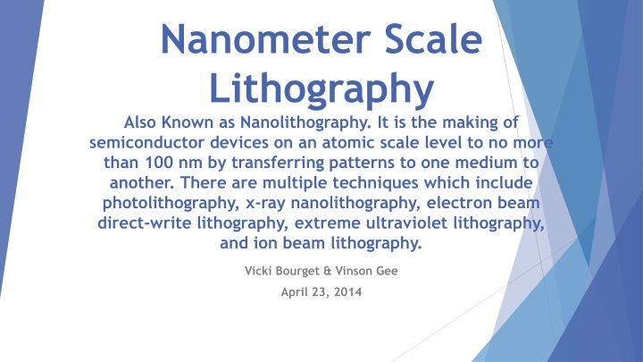
Nanometer Scale Lithography Also Known as Nanolithography. It is the making of semiconductor devices on an atomic scale level to no more than 100 nm by transferring patterns to one medium to another. There are multiple techniques which include photolithography, x-ray nanolithography, electron beam direct-write lithography, extreme ultraviolet lithography, and ion beam lithography. Vicki Bourget & Vinson Gee April 23, 2014
Outline Basic Components Photolithography X-ray nanolithography Electron Beam Direct-Write Lithography Extreme Ultraviolet Lithography Charged Particle Lithography
Optical Lithography Basic Components Source Condenser Collects the source radiation and directs it onto the mask Mask Contains the pattern to be printed on the wafer Reduction imaging lens Projects an image of the mask onto the silicon wafer
Photolithography Uses light to transfer a pattern from photomask to a photoresist chemical on the substrate Chemical treatments engraves the exposure pattern into the material under the photoresist Most cost effective Requires a flat substrate Image From: Lin
X-Ray Nanolithography Selectively remove parts of a thin film Uses x-rays to transfer pattern from mask to photoresist on the substrate Requires special mask sensitive to x-rays Used for batch processing Image From: Antony
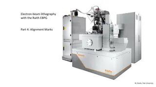
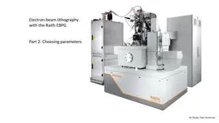
Electron Beam Direct Write Lithography Electron beam Lithography has the ability to fabricate patterns that have nanometer feature sizes Short wavelength and reasonable energy densities Direct writing is the most common approach for electron beam lithography Most often used in mask making, prototyping, fabrication of special small volume products, and research and development for advanced applications Not often used in mass production due to a speed limitation
Electron Beam Direct Write Lithography Direct writing consists of a source of electrons, a focusing optics set, a blanker to turn the beam on and off, a deflection system for moving the beam and a stage for holding the substrate (Image from Ampere)
Electron Beam Direct Write Lithography It is the most desirable process because it is capable of superior resolution and requires no expansive projection optics or time consuming mask production Two types of beams used Gaussian round beam that moves with the wafer to expose the wafer one pixel at a time Can be classified as vector scans Variable shaped beam uses parallel electron beams to write a primitive shape in one shot More speed is gained but the resolution is sacrificed Speed vs detail
Extreme Ultra Violet Lithography Uses a laser-produced plasma source of radiation, a reflective mask and a 4x all reflective imaging system Ideal for creating a high volume of integrated circuits using wavelengths below 100 nm EUVL manufacturing must be done in a vacuum using reflective mirrors and masks since all materials strongly absorb ultraviolet light
Extreme Ultra Violet Lithography This image shows a simple EUVL process where the radiation from the laser-produced plasma illuminates a mask onto the silicon wafer substrate where the IC s are built (Image from Stulen)
Ion Beam Lithography Similar to electron beam lithography, but the key difference is that ion lithography uses heavier, charged ions Heavier ion particles have more momentum and offers high resolution patterning than UV, x-ray, or electron beam lithography Uses include nanometer pattern fabrication and direct doping of the substrate Boron and Phosphorus ions are commonly used
Ion Beam Lithography There are several methods of ion beam lithography Focused ion beam lithography (FIB) Masked ion beam lithography (MIB) Ion beam projection lithography (IBP)
Summary Nanolithography is the making of semiconductor devices on an atomic level to no more that 100 nm Used to create small integrated circuits and printed circuit boards They are still improving the techniques
References Ampere A. Tseng, Kuan Chen, Chii D. Chen, Kung J. Ma, Electron Beam Lithography in Nanoscale Fabrication: Recent Development, IEEE Transactions on Electronics Packaging Manufacturing, Vol. 26, No. 2, April 2003, p. 141-149, PDF Antony Bourdillon and Yuli Vladimirsky, X-ray Lithography on the Sweet Spot , UHRL, San Jose, (2006) Lin, B. J., "Optical Lithography", SPIE Press, Bellingham, WA, 2009, p. 136. Okazaki, Shinji, Comparison of Optical, X-ray, Electron and Ion Beam Lithography, Microelectronic Engineering 9 (1989), p. 297-304, North-Holland, PDF. Stulen, Richard H. and Donald W. Sweeney, Extreme Ultraviolet Lithography, IEEE Journal of Quantum Electronics, Vol. 35, No. 5, May 1999, p. 694 699, PDF
Key Concepts Basic components for lithography are source, condenser, mask, and reduction imaging lens. Photolithography is the most cost effective technique. Most common application is integrated circuits. Electron beam uses either round beam or variable shaped beam. EUV is ideal for creating a high volume of integrated circuits using wavelengths below 100 nm.