On-Chip Superconducting Kinetic Inductance Fourier Transform Spectrometer for mm-Astronomy
This innovative on-chip spectrometer offers a compact solution for mm-wave astronomy research, utilizing superconducting kinetic inductance technology. Learn about the motivation behind its development, the concept of kinetic inductance in superconductors, and the advancements in non-linear kinetic inductance. Explore circuit designs and unique characteristics of the system, providing insights into the future of submm focal planes and calibration technologies.

Uploaded on Feb 26, 2025 | 0 Views
Download Presentation

Please find below an Image/Link to download the presentation.
The content on the website is provided AS IS for your information and personal use only. It may not be sold, licensed, or shared on other websites without obtaining consent from the author.If you encounter any issues during the download, it is possible that the publisher has removed the file from their server.
You are allowed to download the files provided on this website for personal or commercial use, subject to the condition that they are used lawfully. All files are the property of their respective owners.
The content on the website is provided AS IS for your information and personal use only. It may not be sold, licensed, or shared on other websites without obtaining consent from the author.
E N D
Presentation Transcript
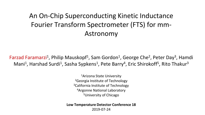
An On-Chip Superconducting Kinetic Inductance Fourier Transform Spectrometer (FTS) for mm- Astronomy Farzad Faramarzi1, Philip Mauskopf1, Sam Gordon1, George Che2, Peter Day3, Hamdi Mani1, Harshad Surdi1, Sasha Sypkens1, Pete Barry4, Eric Shirokoff5, Rito Thakur3 1Arizona State University 2Georgia Institute of Technology 3California Institute of Technology 4Argonne National Laboratory 5University of Chicago Low Temperature Detector Conference 18 2019-07-24
Motivation S. Clesse et al. P. Serra et al. Cosmic Microwave Background spectral distortions (CMB-SD) Structure formation Dissipation of primordial density fluctuations Line Intensity Mapping Epoch of reionization Formation and evolution of ionizing sources on large scales Novel on-chip calibration technology for submm focal planes
Kinetic Inductance of Superconductors Kinetic Inductance Geometric Inductance Normal Resistance Two-fluid Model BCS model Londons Two-Fluid Model of superconductors Zero DC-resistance AC dissipation Inductance Geometric inductance Kinetic inductance Bardeen-Cooper-Schrieffer Description of Superconductivity Cooper pairs Kinetic inductance of superconducting films t
Non-linear Kinetic Inductance Non-linear Kinetic Inductance Characteristic current Function of DC current Materials Niobium nitride Niobium titanium nitride
On-Chip Superconducting FTS output input I STL Geometric Inductance STL Coupling probes /Antenna Schematic of an on-chip FTS Capacitance per unit length Characteristic impedance of STLs ------> Phase velocity --------------------------------------------> Circuit diagram of an on-chip FTS Phase shift
Circuit Design 1 inch Inverted Microstrip Line Geometry Superconducting Meander TLS Two Superconducting Transmission Lines (STLs) Inverted microstrip line geometry Silicon substrate 520 mm long Superconducting probes Two polarizations
Waveguide Coupling 3.4 mm Top view Bottom view Coupling Efficiency of the Waveguide to the Chip Simulated response of the probes Port 1 is waveguide input and port 2 is one of the TLs. Optimization for maximum Coupling Height of probes backshort Thickness of silicon substrate above the probes
Results Optimum coupling to probes with 25 m < Si Thickness < 40 m Optimum back-short thickness is 0.46 mm We only etch area above the probe to gain maximum coupling Simulation of Coupling Efficiency of the Probes vs. Frequency of the new design
Transmission between Waveguides Mode #1 Waveguide #1 Mode #2 Two perpendicular modes in each waveguide Waveguide #2 One set of probes are connected Other probes are terminated at 50 ohms We are interested in understanding of transmission of different modes
Results Transmission simulation modes waveguides Mode#1 has almost 100% transmission band Mode #2 has very little transmission termination Also cross talk between modes is minimal of in the across W- due to Simulation of Transmission across the W-band (75GHz - 110 GHz)
Summary and Future Work Summary We have designed and simulated and Superconducting on-chip Fourier transform spectrometer for sub-mm and mm astronomy We have a design and test setup to couple the FTS chip to the waveguides Future Work Measure phase shift of fabricate Nb, NbN and NbTiN chips Demonstrate the performance of antenna coupled FTS Demonstrate the performance of antenna coupled KID detector FTS Design an array of FTSs