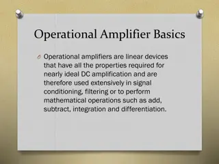
Explore the fundamentals of operational amplifiers (OpAmps) in integrated circuits, including their role as circuit components, feedback mechanisms, and behavior under different conditions. Gain insights into how OpAmps function in both positive and negative feedback circuits and their impact on input and output voltages.
Please find below an Image/Link to download the presentation.
The content on the website is provided AS IS for your information and personal use only. It may not be sold, licensed, or shared on other websites without obtaining consent from the author. If you encounter any issues during the download, it is possible that the publisher has removed the file from their server.
You are allowed to download the files provided on this website for personal or commercial use, subject to the condition that they are used lawfully. All files are the property of their respective owners.
The content on the website is provided AS IS for your information and personal use only. It may not be sold, licensed, or shared on other websites without obtaining consent from the author.
Operational Amplifier as a circuit component Let us consider that the output voltage is inside the operation range (is not limited to Vdd or ground) If we use the basic OpAmp model ??= ?0???? ???? We can express the input differential voltage as ???? ????=?? ?0 If the gain is large enough, the difference between the input voltages will be very small, independent on the output voltage value. ?? ?0 lim ? ???? ???? = lim = 0 ? So, as long at the output voltage is inside the operation range, the input voltages are practically equal.
Operational Amplifier as a circuit component Positive Feedback Negative Feedback Circuit is described by: Circuit is described by: ??=A ?? ?? ??=A ?? ?? ??= ?? ??= ? ??, ??= ?? ??= ? ??, ??=? ? ?? A ?? ??=A ?? ? ? ?? ? ? 1 ??= A ?? ? ? + 1 ??= A ?? ? ? 1 ?? ?? A ? ? + 1 ?? ?? A ??= ??= ? ?
Operational Amplifier as a circuit component ??(?) = ??(?) ?? ?? ? ?? Positive Feedback To simplify the problem we will use f=1 as an example. We shall also consider that there is a finite propagation time. The output is not immediately equal to A times the differential input but tries to reach this value following an exponential response. We consider an initial positive displacement from the equilibrium position, Vd1. The output will exponentially converge towards AVd1 that is a pretty large (as A is large) positive value. This means that the output voltage will move away from the equilibrium position, the differential voltage will increase leading in turn to an ever larger output voltage and even large differential voltage. A similar thing happens if we start with a negative displacement, but this time towards negative output voltages. In both cases, the output moves away from the equilibrium position.
Operational Amplifier as a circuit component ??? = ?? ??(?) ?? ? ?? Negative Feedback We keep the f=1 and finite propagation time assumptions. We consider the same initial displacement, Vd1. The output will exponentially converge towards AVd1 this time this is a large (as A is large) negative value. This means that the output voltage will move towards the equilibrium position, the differential voltage will decrease leading in turn to an smaller but still negative output voltage, resulting in an even smaller displacement. A similar thing happens if we start with a negative displacement. In both cases, the output moves towards the equilibrium position.
Operational Amplifier as a circuit component Both a positive and a negative system have an equilibrium point inside VO range (VO not stuck at supply or ground). For a positive feedback system, this equilibrium position is unstable. Any perturbation from this equilibrium will throw the system towards one of the supply voltages, depending on the direction of the perturbation. For a negative feedback system, this equilibrium position is stable. If a perturbation occurs and takes the system out of equilibrium, it will return to equilibrium by itself. Positive Feedback Negative Feedback
Operational Amplifier as a circuit component Now let us see if the supply can be a stable point. For simplicity, we assume a symmetric supply between Vdd and Vdd. We consider positive feedback first. Positive Feedback First we assume that VO=Vdd and check if there is a Vi range for which this assumption is consistent. In this case Vp=fVdd. VO=Vdd if Vinm<Vinp (we consider A high enough o neglect Vdd/2A). We get: ??< ???? ??= ??? Then we assume that VO= Vdd and check if there is a Vi range for which this assumption is consistent. In this case Vp= fVdd. VO= Vdd if Vinm>Vinp (we consider A high enough o neglect Vdd/2A). We get: ??> ???? ??= ??? To this, we add the unstable equilibrium point determined earlier: ? ? 1 ?? ?? A ??= ?
Operational Amplifier as a circuit component ??< ???? In this case we have only one solution: ??= ??? ??< ???? is fulfilled and ??> ???? is not fulfilled. The unstable solution, VO=Vi/f, would result in output voltage below ??? so it is not an acceptable solution. ??> ???? In this case we have only one solution: ??= ??? ??> ???? is fulfilled and ??< ???? is not fulfilled. The unstable solution, VO=Vi/f would result in output voltage above ??? so it is not an acceptable solution. ????< ??< ???? In this case the system can be in either one of the two stable solutions, ??= ??? and ??= ???, depending on the initial condition. Both ??> ???? and ??< ???? are fulfilled. The unstable solution, marked with a red line, is also present but it is unstable. Any perturbation will push the system out of this state so it can be safely ignored. The system behaves as a hysteresis comparator.
Operational Amplifier as a circuit component Now let us see if the supply can be a stable point. For simplicity, we assume a symmetric supply between Vdd and Vdd. We will now consider the negative feedback case. Negative Feedback First we assume that VO=Vdd and check if there is a Vi range for which this assumption is consistent. In this case Vm=fVdd. VO=Vdd if Vinp>Vinm (we consider A high enough o neglect Vdd/2A). We get: ??> ???? ??= ??? Then we assume that VO= Vdd and check if there is a Vi range for which this assumption is consistent. In this case Vm= fVdd. VO= Vdd if Vinp<Vinm (we consider A high enough o neglect Vdd/2A). We get: ??< ???? ??= ??? To this, we add the solution corresponding to VO inside the operation range (solution that in this case is stable): ? ?+1 ?? ?? A ??= ?
Operational Amplifier as a circuit component ??< ???? In this case we have the solution: ??= ??? ??< ???? is fulfilled and ??> ???? is not fulfilled. The VO=Vi/f solution would result in output voltage below ??? so it is not an acceptable solution. ??> ???? In this case we have the solution: ??= ??? ??> ???? is fulfilled and ??< ???? is not fulfilled. The VO=Vi/f solution would result in output voltage above ??? so it is not an acceptable solution. ????< ??< ???? In this case only the VO=Vi/f solution is acceptable. Both ??> ???? and ??< ???? are not fulfilled. The VO=Vi/f solution gives results in the acceptable range. The system behaves as an amplifier with gain 1/f.
Operational Amplifier as a circuit component OpAmp in negative feedback loop model: ????= ???? ????= ????= 0 Interpretation: An OpAmp in a negative feedback loop will provide the right output voltage such that the negative input will follow the positive input. Comments The negative feedback assumption is necessary so that the output voltage stays in the operation range. We have already seen that having Vo in the operation range and a large enough gain results in the Vinp=Vinm. But this is very unlikely to happen unless a negative feedback loop actively keeps the circuit in a stable point. All OpAmp topologies studied in this lecture have the inputs on gate pins (standard differential pair). This directly results in the Iinp=Iinm=0 condition. We will postulate this condition for the ideal OpAmp. The ideal OpAmp (described by the above model) has infinite output current capability. (This may not be obvious, but it is implied by the above equations the OpAmp will provide the needed VO to fulfill Vinp=Vinm, with no constraint on the output current.) This is obviously not the case for real OpAmps. While negative reaction is needed to keep the output inside the operation range, it may not be sufficient for all input voltages it is very likely that, for some input voltages, the VO voltage given by the above model will result outside the output voltage range. In this case the output voltage will be limited by the supply. (see above example)
Operational Amplifier as a circuit component Offset Voltage For an ideal OpAmp, the output voltage is 0 if the inputs are equal (equilibrium position). Due to either systematic or random mismatches, this is almost never the case for a real OpAmp. We can define the output equivalent offset voltage as the output voltage corresponding to equal input voltages. ??????= ???? = ???,??? ??=A ???? ???? + ???,??? This is however not a very useful definition. As the gain is usually very large, even small mismatches will result in the output voltage being saturated (to either Vdd or Vss). For this reason, a more useful parameter is the input referred offset voltage defined as the differential voltage that needs to be applied at the input to bring the output to the equilibrium position. ??= 0 ???? ????= ??? ??=A ???? ???? ??? Combining the two definitions, we get: ???,???= ? ??? But this is in most cases inaccurate as AVOS is above supply (or below ground).
Operational Amplifier as a circuit component Systematic offset is predictable but it generally is very small as it can be reduced by design techniques. The random offset is in most cases dominant. The random offset is a random variable with 0 mean value. It is (usually) normally distributed. Circuit and layout techniques can be applied to reduce the offset dispersion.
Operational Amplifier as a circuit component Common Mode Gain An ideal OpAmp has zero common mode gain perfect common mode rejection. A real OpAmp will have a small (but finite) common mode gain. ????+ ???? 2 ??= A ???? ???? + ??? Power Supply Rejection For an ideal OpAmp, the output voltage is not influenced by supply voltage variations. A real OpAmp will have a finite power supply rejection. ??=A ???? ???? + ???????
Operational Amplifier as a circuit component Combining all effects, we get ??= A ???? ???? ??? +??? ????+ ???? 2 + ??? + ??????? 2 Common mode gain Supply rejection Ideal OpAmp Offset Asymmetric supply As before, we can solve for the input differential voltage: ????+ ???? 2 +???? ???? ????= ???+1 ?? ??? ??? ??? A 2 ? ? This equation shows that all non-ideal effects presented above (finite gain, common mode and supply rejection) can be included in the offset voltage. If A is large enough, all terms except VOS become negligible. The OpAmp in negative feedback loop model, taking the offset voltage into account is: ???? ????=??? ????= ????= 0
Operational Amplifier as a circuit component Inverting Amplifier As the OpAmp input current is zero, the currents through the two resistors are equal. The opamp is in negative feedback loop, so we consider the input voltages equal Vinp=Vinm. As Vinp=0 it results that Vinm=0 (virtual ground). The circuit is described by: ? =?? 0 =0 ?? ?1 ?2 ?? ?1 = ?? ?2 ??= ?2 ?1?? This circuit will never work as presented in an asymmetric supply as either Vi or VO results below ground. The most common solution is to refer the circuit to Vdd/2 (Vinp=Vdd/2 instead of ground).
Operational Amplifier as a circuit component Non Inverting Amplifier As the OpAmp input current is zero, the currents through the two resistors are equal. The opamp is in negative feedback loop, so we consider the input voltages equal Vinp=Vinm. As Vinp=Vi it results that Vinm=Vi. The circuit is described by: ? =?? =?? ?? ?1 ?2 ?2??= ?1?? ?1?? ?1??= ?1+ ?2?? ??= 1 +?2 ?? ?1