Output Stage Design for Operational Amplifiers and Microelectronic Systems
"Explore output stages for operational amplifiers, gain reduction due to loading, specifications, example op-amp models, and class A output stages. Learn about current sources, voltage swings, and more in microelectronic system design."

Download Presentation

Please find below an Image/Link to download the presentation.
The content on the website is provided AS IS for your information and personal use only. It may not be sold, licensed, or shared on other websites without obtaining consent from the author. If you encounter any issues during the download, it is possible that the publisher has removed the file from their server.
You are allowed to download the files provided on this website for personal or commercial use, subject to the condition that they are used lawfully. All files are the property of their respective owners.
The content on the website is provided AS IS for your information and personal use only. It may not be sold, licensed, or shared on other websites without obtaining consent from the author.
E N D
Presentation Transcript
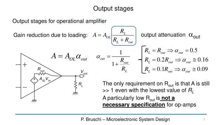
Output stages Output stages for operational amplifier R + output attenuation out = A A L Gain reduction due to loading: OL R R L out = = = = 0.5 R R R R 1 R R = A L out out A = 0.2 0.1 0.16 0.09 R R OL out out + L out out 1 out L L out out The only requirement on Routis that A is still >> 1 even with the lowest value of RL A particularly low Rout is not a necessary specification for op-amps P. Bruschi Microelectronic System Design 1
Example of commercial op-amp with high output resistance 315 10 3 RL=500 k A A OL 1 R R A = 55 10 3 RL=10 k A = = 0.176 R out A + 1 out OL 0.21 R 0.21 47k R R L out L out L P. Bruschi Microelectronic System Design 2
Specifications for an output stage Currents (sink and source) I I I max max ON Sink out OP Source Vout-max Voltages (swing) = = + V V V V V V Vout-min max out dd H min out ss L The output swing depends on the currents the stage has to feed to the load P. Bruschi Microelectronic System Design 3
Examples OPA 377 (Analog Devices) Linear Tech. P. Bruschi Microelectronic System Design 4
Output stage classes Simple model of an output stage constant Idev2 By subtracting two unipolar currents, we obtain a bi- directional output current = I I I 1 2 out dev dev P. Bruschi Microelectronic System Design 5
Typical class A case: low power efficiency = I I I 1 2 out dev dev In a class-A stage, one of the two output devices operates at constant current The maximum symmetrical current coincides with Idev 2, which is a constant bias current. Therefore, the maximum (symmetrical) output current is smaller than the quiescent current absorption. P. Bruschi Microelectronic System Design 6
Class A source followers The n-MOS source follower can be used as a negative voltage-shifter = V V V V out in GS V in dd V V V Because the circuit that produces Vin(driver) uses the same Vdd out dd GS V = V V GS H GS The large margin to to Vddmakes it not suitable for rail-to-rail output stages (practically mandatory in modern, low voltrage applications) P. Bruschi Microelectronic System Design 7
P-type Source follower The p-MOS source follower can be used as a positive voltage shifter. = + V V V out V in V GS V in ss GS + V V V out ss GS Margin to Vss (too large for typical supply voltages used in modern CMOS processes) = V V L GS P. Bruschi Microelectronic System Design 8
Class-A source followers: output current limits The positive output current (IOP) is limited only by the MOSFET size I I 0 OP The negative output current (ION) is limited by I0, which is the quiescent supply current opposite condition: it is the positive current to be limited by I0, I I 0 ON n source follower p source follower P. Bruschi Microelectronic System Design 9
Source followers: summary N-type: Large margin with respect to Vdd Sink current limited by bias current P-type: Large margin with respect to Vss Source current limited by bias current Class AB source followers (push-pull stages) remove the limitation on the output current but impose a large margin with respect to both rails (Vdd, Vss) Source followers are avoided in amplifiers designed for low supply voltages and for large output swing P. Bruschi Microelectronic System Design 10
Common source output stages: class-A case Margins to the rails are now only a VDSAT, which is much smaller than a VGS. The common source output stage has a practically rail-to-rail output swing + V DSATn V V V DSATp V ss out dd P. Bruschi Microelectronic System Design P. Bruschi Microelectronic System Design 11 11
Small signal properties of the class-A common source stage R = A A L V VO + R R ( ) out L = = // A g r r The unipolar common source is a gain stage (inverting) that can be used also as output stage VO mn // dn dp ( ) R r r out dn dp P. Bruschi Microelectronic System Design P. Bruschi Microelectronic System Design 12 12
Class-A common source: maximum output current n-version = = + (0) V V v -VGSp in in in I I I out Dp Dn I0 = (0) V I I in Dn Dp = = I I constant I0 0 Dp = I I ON MAX = 0 I I OP MAX class-A 0 VGSn class-A p-version: (the input signal is invariant when referred to Vdd) The input voltage is invariant to the supply voltages when it is referred to Vss: the preceding stage should provide an output with the same property P. Bruschi Microelectronic System Design 13
Class-AB common source: principle of operation class-AB control push (driver) operating point Mp turns off pull = Mn turns off V I I I in out Dp Dn P. Bruschi Microelectronic System Design 14 14
Class-AB common-source output stages: maximum output currents V ( ) 2 GSp p I GSp MAX V V OP MAX tp 2 ( ) 2 n I GSn MAX V V ON MAX tn 2 GSp MAX V V V p , n Driver max GSn GSn Different topologies are available for the class-AB driver. They differ for the maximum VGSthat can be delivered to Mpand Mnand for the minimum supply voltage P. Bruschi Microelectronic System Design 15 15
Class-AB common-source output stages: equivalent voltage source Vdd = constant V V Vgp gp gn Mp VB Vout Vgn Mn This is equivalent to have a voltage source (battery) across the two gates. Vss = = v v v For small signals: gn gp in P. Bruschi Microelectronic System Design 16
Class-AB common-source output stages: small signal gain ) ( // vgnand vgpmust have the same sign to produce in-phase effects on vout = R + v R = mn gn g v r mp gp g v out out r out dn dp = = v v v For: ( g gn gp in ( ) ) = + A g g R = + v R g v VO mn mp out out out mn mp in P. Bruschi Microelectronic System Design 17
Two-stage operational amplifiers: examples P. Bruschi Microelectronic System Design 18
Two-stage operational amplifier with class-AB output stage Vgp = = V V V V 10 gp gn B GS Vgn P. Bruschi Microelectronic System Design 19