Overview of Memory Hierarchy in Computer Systems
This review covers the importance of memory systems in single processor performance, the typical memory hierarchy components, and the challenges faced by real-world uniprocessors. Explore the impact of caches, local memory, and the role of compilers and hardware optimization in enhancing program efficiency.
Download Presentation

Please find below an Image/Link to download the presentation.
The content on the website is provided AS IS for your information and personal use only. It may not be sold, licensed, or shared on other websites without obtaining consent from the author.If you encounter any issues during the download, it is possible that the publisher has removed the file from their server.
You are allowed to download the files provided on this website for personal or commercial use, subject to the condition that they are used lawfully. All files are the property of their respective owners.
The content on the website is provided AS IS for your information and personal use only. It may not be sold, licensed, or shared on other websites without obtaining consent from the author.
E N D
Presentation Transcript
Caches and Memory Hierarchy: Review UCSB CS240A, Winter 2016 1
Motivation Most applications in a single processor runs at only 10- 20% of the processor peak Most of the single processor performance loss is in the memory system Moving data takes much longer than arithmetic and logic Parallel computing with low single machine performance is not good enough. Understand high performance computing and cost in a single machine setting Review of cache/memory hierarchy 2
Typical Memory Hierarchy On-Chip Components Control Third- Level Cache (SRAM) Secondary Memory (Disk Or Flash) Cache Main Memory (DRAM) Instr Second- Level Cache (SRAM) Datapath RegFile Cache Data Speed (cycles): s 1 s 10 s 100 s 1,000,000 s Size (bytes): 100 s 10K s M s G s T s Cost/bit: highest lowest Principle of locality + memory hierarchy presents programmer with as much memory as is available in the cheapest technology at the speed offered by the fastest technology 3
Idealized Uniprocessor Model Processor names bytes, words, etc. in its address space These represent integers, floats, pointers, arrays, etc. Operations include Read and write into very fast memory called registers Arithmetic and other logical operations on registers Order specified by program Read returns the most recently written data Compiler and architecture translate high level expressions into obvious lower level instructions Read address(B) to R1 Read address(C) to R2 R3 = R1 + R2 Write R3 to Address(A) A = B + C Hardware executes instructions in order specified by compiler Idealized Cost Each operation has roughly the same cost (read, write, add, multiply, etc.) 4
Uniprocessors in the Real World Real processors have registers and caches small amounts of fast memory store values of recently used or nearby data different memory ops can have very different costs parallelism multiple functional units that can run in parallel different orders, instruction mixes have different costs pipelining a form of parallelism, like an assembly line in a factory Why is this your problem? In theory, compilers and hardware understand all this and can optimize your program; in practice they don t. They won t know about a different algorithm that might be a much better match to the processor 5
Memory Hierarchy Most programs have a high degree of locality in their accesses spatial locality: accessing things nearby previous accesses temporal locality: reusing an item that was previously accessed Memory hierarchy tries to exploit locality to improve average processor control Second level cache (SRAM) Secondary storage (Disk) Main memory Tertiary storage datapath (DRAM) (Disk/Tape) on-chip cache registers Speed 1ns 10ns 100ns 10ms 10sec Size KB MB GB TB PB 6
Review: Cache in Modern Computer Architecture Memory Processor Input Control Program Cache Datapath Address Bytes PC Write Data Registers Data Arithmetic & Logic Unit (ALU) Read Data Output Processor-Memory Interface I/O-Memory Interfaces 7
Cache Basics Cache is fast (expensive) memory which keeps copy of data in main memory; it is hidden from software Simplest example: data at memory address xxxxx1101 is stored at cache location 1101 Memory data is divided into blocks Cache access memory by a block (cache line) Cache line length: # of bytes loaded together in one entry Cache is divided by the number of sets A cache block can be hosted in one set. Cache hit: in-cache memory access cheap Cache miss: Need to access next, slower level of cache 8
Memory Block-addressing example 3/17/2025 9
Processor Address Fields used by Cache Controller Block Offset: Byte address within block B is number of bytes per block Set Index: Selects which set. S is the number of sets Tag: Remaining portion of processor address Processor Address Block offset Set Index Tag Size of Tag = Address size log(S) log(B) Cache Size C = Associativity N # of Set S Cache Block Size B Example: Cache size 16K. 8 bytes as a block. 2K blocks If N=1, S=2K using 11 bits. 10
Block number aliasing example 12-bit memory addresses, 16 Byte blocks Block # Block # mod 2 Block # mod 8 1-bit set index 3-bit set index 3/17/2025 11
Direct-Mapped Cache: N=1. S=Number of Blocks=210 4byte blocks, cache size = 1K words (or 4KB) Byte offset 31 30 . . . 13 12 11 . . . 2 1 0 Tag 20 Index 10 Data Hit Valid bit ensures something useful in cache for this index Read data from cache instead of memory if a Hit Index Valid Tag Data 0 1 2 . . . 1021 1022 1023 Compare Tag with upper part of Address to see if a Hit 32 20 Comparator Cache Size C = Associativity N # of Set S Cache Block Size B 12
Cache Organizations Fully Associative : Block can go anywhere N= number of blocks. S=1 Direct Mapped : Block goes one place N=1. S= cache capacity in terms of number of blocks N-way Set Associative : N places for a block Block ID Block ID 13
Four-Way Set-Associative Cache 28 = 256 sets each with four ways (each with one block) 31 30 . . . 13 12 11 . . . 2 1 0 Byte offset Set Index 22 Tag 8 Index V Tag V Tag V Tag V Tag Data Data Data Data 0 1 2 0 1 2 0 1 2 0 1 2 Way 0 Way 1 Way 2 Way 3 . . . . . . . . . . . . 253 254 255 253 254 255 253 254 255 253 254 255 32 4x1 select 14 Hit Data
How to find if a data address in cache? Assume block size 8 bytes last 3 bits of address are offset. Set index 2 bits. 0b1001011 Block number 0b1001. Set index 2 bits (mod 4) Set number 0b01. Tag = 0b10. If directory based cache, only one block in set #1. If 4 ways, there could be 4 blocks in set #1. Use tag 0b10 to compare what is in the set. 15
Cache Replacement Policies Random Replacement Hardware randomly selects a cache evict Least-Recently Used Hardware keeps track of access history Replace the entry that has not been used for the longest time For 2-way set-associative cache, need one bit for LRU replacement Example of a Simple Pseudo LRU Implementation Assume 64 Fully Associative entries Hardware replacement pointer points to one cache entry Whenever access is made to the entry the pointer points to: Move the pointer to the next entry Otherwise: do not move the pointer (example of not-most-recently used replacement policy) Entry 0 Entry 1 Replacement : Pointer 16 Entry 63
Handling Stores with Write-Through Store instructions write to memory, changing values Need to make sure cache and memory have same values on writes: 2 policies 1) Write-Through Policy: write cache and write through the cache to memory Every write eventually gets to memory Too slow, so include Write Buffer to allow processor to continue once data in Buffer Buffer updates memory in parallel to processor 17
Write-Through Cache Write both values in cache and in memory Write buffer stops CPU from stalling if memory cannot keep up Write buffer may have multiple entries to absorb bursts of writes What if store misses in cache? Processor 32-bit Address 32-bit Data Cache 12 252 99 7 1022 131 2041 Write Buffer 20 Addr Data 32-bit Address 32-bit Data Memory 18
Handling Stores with Write-Back 2) Write-Back Policy: write only to cache and then write cache block back to memory when evict block from cache Writes collected in cache, only single write to memory per block Include bit to see if wrote to block or not, and then only write back if bit is set Called Dirty bit (writing makes it dirty ) 19
Write-Back Cache Processor Store/cache hit, write data in cache only & set dirty bit Memory has stale value Store/cache miss, read data from memory, then update and set dirty bit Write-allocate policy Load/cache hit, use value from cache On any miss, write back evicted block, only if dirty. Update cache with new block and clear dirty bit. 32-bit Address 32-bit Data Cache 12 252 D D D D 99 7 1022 131 2041 Dirty Bits 20 32-bit Address 32-bit Data Memory 20
Write-Through vs. Write-Back Write-Through: Simpler control logic More predictable timing simplifies processor control logic Easier to make reliable, since memory always has copy of data (big idea: Redundancy!) Write-Back More complex control logic More variable timing (0,1,2 memory accesses per cache access) Usually reduces write traffic Harder to make reliable, sometimes cache has only copy of data 21
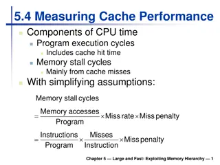
Cache (Performance) Terms Hit rate: fraction of accesses that hit in the cache Miss rate: 1 Hit rate Miss penalty: time to replace a block from lower level in memory hierarchy to cache Hit time: time to access cache memory (including tag comparison) 22
Average Memory Access Time (AMAT) Average Memory Access Time (AMAT) is the average time to access memory considering both hits and misses in the cache AMAT = Time for a hit + Miss rate Miss penalty Given a 0.2ns clock, a miss penalty of 50 clock cycles, a miss rate of 2% per instruction and a cache hit time of 1 clock cycle, what is AMAT? AMAT = 1 cycle + 0.02*50 = 2 cycles = 0.4ns. 23
