PCB Assignment Recap and Soldering Logistics Information
Gain insights into the PCB design process, assignment solutions, late submission policy, and upcoming soldering assignment details. Understand the purpose behind PCB and soldering tasks in engineering education with a focus on professional final project demonstrations.

Download Presentation

Please find below an Image/Link to download the presentation.
The content on the website is provided AS IS for your information and personal use only. It may not be sold, licensed, or shared on other websites without obtaining consent from the author. If you encounter any issues during the download, it is possible that the publisher has removed the file from their server.
You are allowed to download the files provided on this website for personal or commercial use, subject to the condition that they are used lawfully. All files are the property of their respective owners.
The content on the website is provided AS IS for your information and personal use only. It may not be sold, licensed, or shared on other websites without obtaining consent from the author.
E N D
Presentation Transcript
PCB Assignment Recap and Soldering Assignment Information March 11, 2022
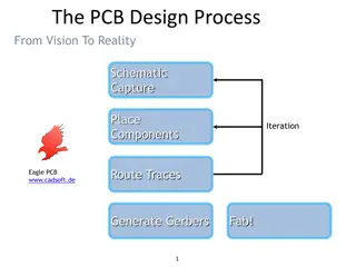
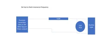
PCB design process step 1: Schematic (abstract)
PCB Assignment Solution Observations Spot check of submissions looks pretty good Please share any feedback you have regarding the assignment Not all students submitted a solution Late policy on assignments: 25% reduction per day late, i.e., Late score = Score 1 25%? where ? is the number of days late
Soldering Assignment Logistics The soldering assignment is an individual assignment (all students must complete the assignment) Due date: Friday, March 11, 5pm Location: Senior design lab (D225) Sign up for a time slot here: https://docs.qq.com/sheet/DR1VKVW5yVVhyeG5V?tab=BB08J2
Soldering Assignment Logistics Complete the assignment and take the (tested) PCB home with you TAs will grade the assignment Today (3.11), 4:00-5:00 PM, D225 Lab Bring your soldered PCB to the lab for and demo it with a TA Who to contact for help: Lab staff: Shilei Zhang and Si Li TAs Course staff
Purpose of the PCB and soldering assignments It is true: you may never construct a PCB or solder an electronic component again in your engineering career A circuit breadboard is useful for prototyping The ultimate goal of senior design is a professional final project demonstration A mess of wires and components gives a poor impression Time and again students scramble to find loose wires and components during live demos
The Design Process 2b. Prototype 2c. Testing / validation 2a. Design 1. Ideation and specification 3. Final demonstration
Breadboards vs. PCBs Conclusions Breadboards are for prototyping PCB design and construction takes some skill: Soldering is not always easy Certain situations (e.g., high power / frequency) offer much greater challenge Compared to UIUC in the USA, we have advantages in China: Rapid turnaround time (days instead of weeks to receive a custom PCB) Low cost


")