PN Junction in Physics at Hindu College Guntur
Explore the concepts of N-Type and P-Type materials, PN Junction, and the effects of biasing in the field of Physics at Hindu College Guntur Department of Physics. Learn about the characteristics, differences, and applications of these materials in electronic devices.

Download Presentation

Please find below an Image/Link to download the presentation.
The content on the website is provided AS IS for your information and personal use only. It may not be sold, licensed, or shared on other websites without obtaining consent from the author. If you encounter any issues during the download, it is possible that the publisher has removed the file from their server.
You are allowed to download the files provided on this website for personal or commercial use, subject to the condition that they are used lawfully. All files are the property of their respective owners.
The content on the website is provided AS IS for your information and personal use only. It may not be sold, licensed, or shared on other websites without obtaining consent from the author.
E N D
Presentation Transcript
HINDU COLLEGE GUNTUR Department of Department of Physics Physics
N-Type Material N-Type Material: When extra valence electrons are introduced into a material such as silicon an n-type material is produced. electrons are introduced impurities or dopant into the silicon. dopant used to create an n-type material are Group V elements. used dopant from Group V are arsenic, antimonyand phosphorus. The extra valence by putting The +4 +4 +4 The most commonly +4 +5 +4 The 2D diagram to the left shows the extra electron that will be present when a Group V dopant is introduced to a material such as silicon. Thisextraelectron is very mobile. +4 +4 +4 3/24/2023 3
P-Type Material P-Type Material: P-type material is produced when the dopant that is introduced is from Group III. III elements have only 3 valence electrons and therefore there is an electron missing. This creates a hole (h+), or a positive charge that can move around Commonly used Group aluminum,boron,and gallium. Group +4 +4 +4 in the material. dopant III are +4 +3 +4 The 2D diagram to the left shows the hole that will be present when a Group III dopant is introduced to a material such as silicon. This hole is quite mobile in the same way the extra electron ismobile in a n-type material. +4 +4 +4 4
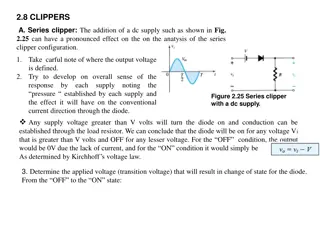
The PN Junction Steady State Metallurgical Junction Na Nd When no external source is connected to the pn junction, diffusion drift balance each other out for both the holes and electrons + + + + + - - - - - + + + + + - - - - - P n and + + + + + - - - - - + + + + + - - - - - Space Charge Region ionized acceptors ionized donors E-Field _ _ + + = = = = h+ drift e-drift h+ diffusion e-diffusion Space Charge Region: Also called the depletion region. This region includes the net positively and negatively charged regions. The space charge region does not have any free carriers. The width of the space charge region is denoted by W in pn junction formula s. Metallurgical Junction: The interface where the p- and n-type materials meet. Na & Nd: Represent the amount of negative and positive doping in number of carriers per centimeter cubed. Usually in the range of 1015to 1020. 5
The Biased PN Junction Metal Contact Ohmic Contact _ + (Rs~0) App lied Field P n Electric I _ + Vapplied The pn junctionis considered biasedwhen an external voltage isapplied. Therearetwo types of biasing: Forwardbiasand Reversebias. Theseare describedon then next slide.
The Biased PN Junction Forward Bias: In forward bias the depletion region shrinks slightly in width. With this shrinking the energy required for charge carriers to cross the depletion region decreases exponentially. Therefore, increases, current starts to flow across the junction. The barrier potential of the diode is the voltage at which appreciable current starts to flow through the diode. Thebarrierpotentialvariesfor differentmaterials. Vapplied> 0 as the applied voltage Reverse Bias: Under reverse bias the depletion region widens. causes the electric field produced by the ions to cancel out the applied reverse bias voltage. current, Is (saturation current) flows under reverse bias conditions. This saturation current is made up of electron-hole pairs being produced in the depletion region. Saturation current is sometimes referred to as scale current because of it s relationship to junction temperature. This A small leakage Vapplied< 0 6
Properties of Diodes Figure1.10 The Diode TransconductanceCurve2 ID VD= BiasVoltage (mA) ID= Currentthrough Diode. IDis Negative for Reverse Bias and PositiveforForward Bias IS VBR IS= Saturation Current VD ~V VBR= Breakdown Voltage V = BarrierPotential Voltage (nA) 7
Properties of Diodes The Shockley Equation The transconductance curve on the previous slideis characterized by the followingequation: ID= IS(eVD/ VT 1) As describedin the last slide, IDis the currentthroughthe diode,ISis the saturationcurrentand VDis the applied biasingvoltage. VTis the thermalequivalent voltage and is approximately 26 mV at room temperature. Theequationto find VTat varioustemperaturesis: VT= kT q k = 1.38 x 10⁻²³J/K T = temperature in Kelvin q = 1.6 x 10⁻¹⁹C is the emission coefficient for the diode. It is determined by the way the diodeis constructed. Itsomewhatvarieswithdiodecurrent. Fora silicondiode is around 2 for low currentsand goes down to about1 at highercurrents
Types of Diodes and Their Uses PN Junction Diodes: Are used to allow current to flow in one direction while blocking current direction. The pn junction diode is the typical diode that has been used in the previouscircuits. flow in the opposite P n A K Schematic Symbol for a PN Junction Diode Representative Structure for a PN Junction Diode Zener Diodes: Are specifically designed to operate under reverse breakdown conditions. These diodes have a very accurateand specificreversebreakdownvoltage. A K Schematic Symbol for a Zener Diode 9
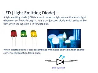
Types of Diodes and Their Uses Light-Emitting Diodes: Light-emitting diodes are designed with a very large band gap so movement of carriers across their depletion region emits photons of light energy. Lower band gap LEDs (Light-Emitting Diodes) emit infrared radiation, while LEDs with higher band gap energy emit visible light. Many stop lights are now starting to use LEDs because they are extremely bright and last longer than regular bulbs for a relativelylowcost. The arrows in the LED representation indicate emitted light. A K Schematic Symbol for a Light-Emitting Diode 11
Types of Diodes and Their Uses Photodiodes: While LEDs emit light, Photodiodes are sensitive to received light. They are constructed so their pn junction can be exposed to the outside through a clearwindowor lens. A K In Photoconductive mode the saturation current increases in proportion to the intensity of the received light. This type of diode is used in CD players. A K In Photovoltaic mode, when the pn junction is exposed to a certain wavelength of light, the diode generates voltage and can be used as an energy source. This type of diode is used in the productionof solar power. Schematic Symbols for Photodiodes 12