Programmable Logic Devices: ROM, PLA, PAL, CPLD, and FPGA Explained
Discover the intricacies of Programmable Logic Devices (PLDs) such as ROM, PLA, PAL, CPLD, and FPGA, which store permanent binary information and utilize different programming methods. Learn about the function synthesis, programming techniques, and structures of these devices in this comprehensive guide.

Uploaded on | 0 Views
Download Presentation

Please find below an Image/Link to download the presentation.
The content on the website is provided AS IS for your information and personal use only. It may not be sold, licensed, or shared on other websites without obtaining consent from the author. If you encounter any issues during the download, it is possible that the publisher has removed the file from their server.
You are allowed to download the files provided on this website for personal or commercial use, subject to the condition that they are used lawfully. All files are the property of their respective owners.
The content on the website is provided AS IS for your information and personal use only. It may not be sold, licensed, or shared on other websites without obtaining consent from the author.
E N D
Presentation Transcript
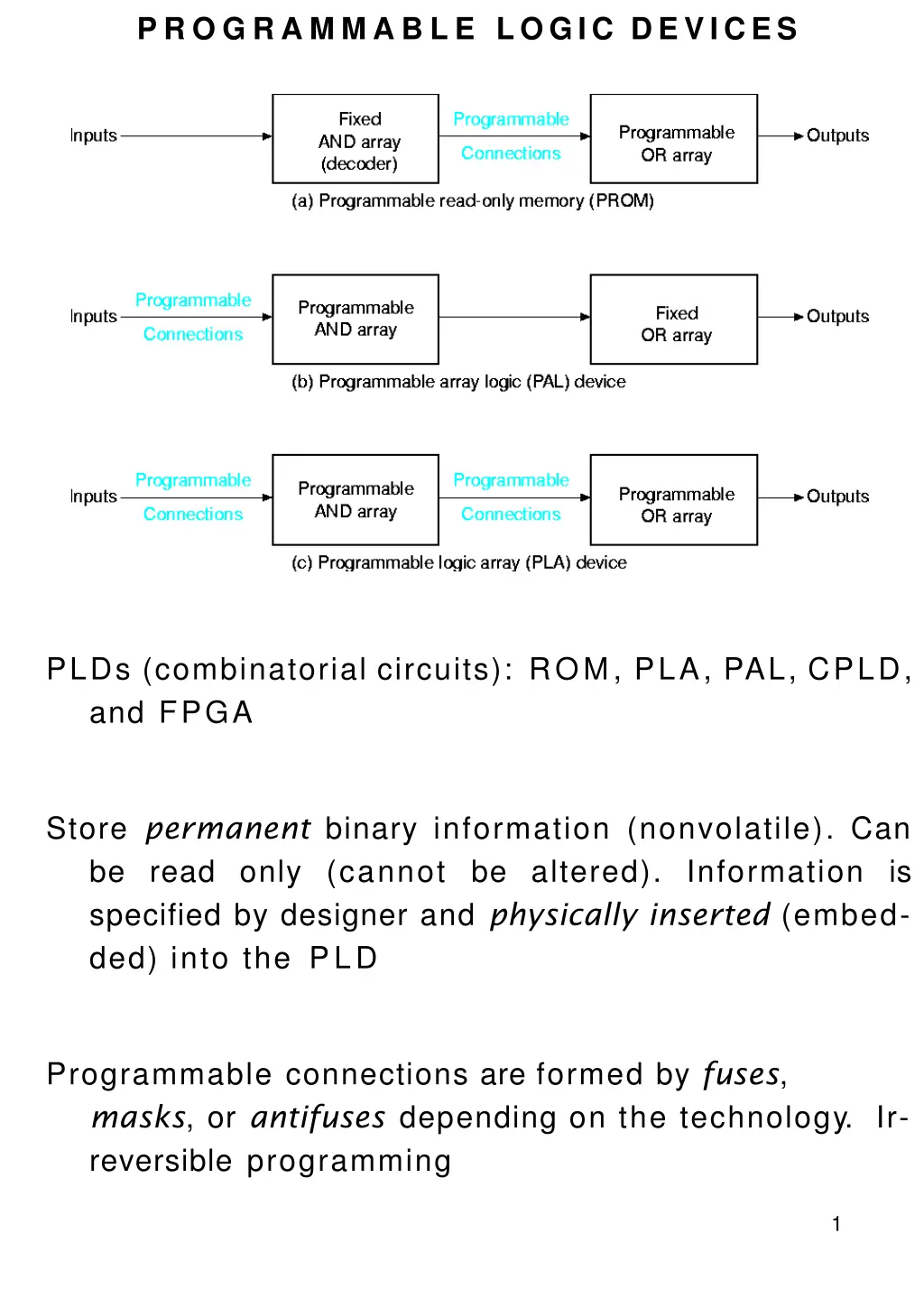
P R O G R A M M A B L E LOGIC DEVICES PLDs (combinatorial circuits): ROM, PLA, PAL, CPLD, and FPGA Store permanent binary information (nonvolatile). Can be read only (cannot be altered). Information is specified by designer and physically inserted (embed- ded) into the PLD Programmable connections are formed by fuses, masks, or antifuses depending on the technology. Ir- reversible programming 1
Read-Only Memory 2k n ROM k inputs (address) n outputs (data) 32 8 ROM k 2k decoder to decode input address n OR gates with 2k input each Decoder output is connected to all n OR gates through fuses ROM 2k n programmable connections 2
Programming a R O M Example of 4 2 ROM NonProgrammed ROM 2 to 4 Decoder I0 D1 D2 D3 D0 Truth table Address I1 I0 0 0 0 1 1 0 1 1 Content A1 0 1 1 1 I1 A0 1 0 1 0 A1 A0 Programmed ROM D0 D1 D2 D3 Compact ROM D0 D1 D2 D3 2 to 4 Decoder 2 to 4 Decoder I0 I0 I1 I1 A1 A0 A1 A0 Truth table address and content of ROM Programming stores truth table in ROM 0 = Open connection = Fuse blown 1 = Closed connection = Fuse intact 3
Function Synthesis with R O M Any set of functions f1(xk, ...,x1), ..., fn(xk, ...,x1) can be realized with a 2k n ROM m(0, 3), Example: Implement f1(x2, x1) = f2(x2, x1) = x2+ x1, and f3(x2, x1) = 4 3 ROM QM (1) with a Truth table Address x2 x1 0 0 0 1 1 0 1 1 Content f3 f2 1 1 0 0 1 0 1 0 f1 1 0 0 1 4 3 ROM storing f1, f2, f3 2 to 4 D0 Decoder D1 D2 D3 x1 x2 f3 f2 f1 4
Programmable Logic Array n inverters m fuses k xm fuses kAND gates mOR gates n x k fuses m inverters moutputs n inputs Behave like a ROM but has different structure Uses ANDs array instead of decoder to produce product terms of inputs Has programmable connections before ANDs, be- tween ANDs and ORs, after ORs. That is 2nk + km + m fuses More flexible than ROM but more difficult to pro- gram Logic expressions for content information to be stored in PLA must be obtained fisrt, then mini- mized, and finally programmed into the PLA using a PLA program table PLA program table specifies product terms and sum terms of information that will be stored in PLA 5
Programming a PLA PLA Program Table Inputs A B 1 1 Outputs F1 1 1 F2 C Term AB AC BC A BC Term# 1 2 3 4 0 1 1 0 1 1 1 1 0 1 T C Corresponding PLA Implementation 6
Function Synthesis with PLA Any set of functions f1(x1, ...,xn), ..., fm(x1, ...,xn) can be realized with a PLA m(3, 5, 6, 7) and Example Implement f1(a, b,c) = f2(a, b,c) = m(0, 2, 4) with a PLA First Simplify f1, f 1, f2, f 2, that is f1, f2 5 terms f1, f 2 4 terms f 1, f2 3 terms f 1, f 2 5 terms f1(a, b,c) = ab+ ac + bc f 1(a,b,c) = a b+ a c + b c f2(a, b, c) = a c + b c f 2(a,b,c) = ab+ c Second Select combination of functions that has less terms, that is f1= f 1= a b+ a c + b c f2(a, b,c) = a c + b c Third Construct functions a PLA program table from selected Inputs a b 0 0 0 0 Outputs f1 1 1 1 C f2 c Term a b a c b c Term# 1 2 3 0 0 1 1 T 7
Function Synthesis with PLA (continued) Third Construct functions a PLA program table from selected Inputs a b 0 0 0 0 Outputs f1 1 1 1 C f2 c Term a b a c b c Term# 1 2 3 0 0 1 1 T Fourth Construct PLA circuit from PLA program table 8
Programmable Array Logic n inverters k AND gates mOR gates n x k fuses n inputs moutputs Similar to PLA Only the connection inputs to ANDs are programmable Easier to program than but not as flexible as PLA There are feedback connections Logic expressions for content information to be stored in PAL must be obtained fisrt, then mini- mized, and finally programmed into the PAL using a PAL program table PAL program table specifies only product terms of information that will be stored in PAL 9
Arithmetic-Logic Unit Essential element of the Central Processing Unit Arithmetic and logic functions on binary words n-bit data inputs A and B n-bit data output tt = f (A, B) Selection inputs S0, S1 select a function f Selection input S2select an operating mode (arith- metic or logic) 11
ALU (continued) Logic Circuit Arithmetic Circuit 12
ALU (continued) 4-bit Arithmetic Circuit 13
ALU (continued) Arithmetic and Logic Circuit 14