Programmable Logic Families and Embedded System Design Overview
This chapter provides an overview of various programmable logic families such as ASIC, PAL, FPGA, CPLD, and SOC. It discusses the concept of user-programmable logic families and their evolution over the years. The chapter delves into Application-Specific Integrated Circuit (ASIC), Full custom vs. Semi-custom designs, and the integration of FPGA with embedded processors like ARM. It also explores programmable logic devices including PLA, PAL, GAL, and CPLD, highlighting their functionalities and applications in the field of embedded system design.

Download Presentation

Please find below an Image/Link to download the presentation.
The content on the website is provided AS IS for your information and personal use only. It may not be sold, licensed, or shared on other websites without obtaining consent from the author.If you encounter any issues during the download, it is possible that the publisher has removed the file from their server.
You are allowed to download the files provided on this website for personal or commercial use, subject to the condition that they are used lawfully. All files are the property of their respective owners.
The content on the website is provided AS IS for your information and personal use only. It may not be sold, licensed, or shared on other websites without obtaining consent from the author.
E N D
Presentation Transcript
Programmable logic families and embedded system design KH Wong CENG3430: Programmable logic v.8a 1
Overview of this chapter What is ASIC ? PAL (Programmable array logic) FPGA (Field-programmable gate array) CPLD (Complex programmable logic device) SOC (system on chip) CENG3430: Programmable logic v.8a 2
Application Specific integrated circuit field (ASIC) ASIC Full custom (ordered by user e.g. TSMC) Semi-custom (designed by user Apple I-phone. To be made by TSMC or Samsung) User programmable logic families 1) PLA (Programmable array logic) 2) PAL (Programmable logic array) 3) GAL (gate array logic ) 4) CPLD (Complex programmable logic device) 5) FPGA (Field-programmable gate array) 6) SOC (system on chip) FPGA + Embedded processor (ARM) CENG3430: Programmable logic v.8a 3
User programmable logic families according to http://en.wikipedia.org/wiki/Programmable_logic_device#PLA 1) PLA (1970) Programmable Logic Array A programmable logic array (PLA) has a programmable AND gate array, which links to a programmable OR gate array, which can then be conditionally complemented to produce an output. E.g. TMS2000 2) PAL (1978) Programmable Array Logic PAL devices have arrays of transistor cells arranged in a "fixed-OR, programmable-AND" plane used to implement "sum-of-products" binary logic equations for each of the outputs in terms of the inputs and either synchronous or asynchronous feedback from the outputs. Example: PAL16R6 CENG3430: Programmable logic v.8a 4
User Programmable logic families (continue) according to http://en.wikipedia.org/wiki/Programmable_logic_device#PLA 3) GALs (1985) Generic array logic E.g. GAL16V8 Each output has an flip flop for making sequential logic or / xor gates /Flip flops Add plane CENG3430: Programmable logic v.8a 5
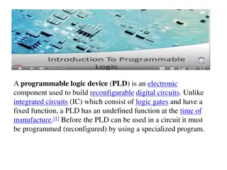
User Programmable logic families (continue) 4) CPLD (1999?) (Complex programmable logic device) e.g. xc9500 from xilinx Non-volatile (program memory still there even after power off) Next page CENG3430: Programmable logic v.8a 6
XC9500 Microcell within function block CENG3430: Programmable logic v.8a 7
User Programmable logic families (continue) 5) FPGA (1988?) (field programmable gate array) E.g. XC4000 from Xilinx, volatile (also has non- volatile versions) CENG3430: Programmable logic v.8a 8
Re-programmable Hardware: FPGA Field Programmable Gate Array So what is inside an FPGA IOB=Input/Output block CLB=Configurable Logic block (static ram based) Change the CLBs to get the desired functions From http://www.alldatasheet.co.kr/datasheet- pdf/pdf_kor/49173/XILINX/XCS10-3PC84C.html CENG3430: Programmable logic v.8a 9
Inside a CLB (Configurable Logic block ) The CLB is a fixed design but you can change the logic function for generating output from input G1-G4 by reprogramming the bits in the logic function lookup table. This will change the overall logic function of the CLB Re-programming the logic table CLB FPGA CLB (Configurable Logic block ) http://www.design-reuse.com/news_img/20100913_1.gif http://pldworld.biz/html/technote/pldesignline/bobz-02.gif CENG3430: Programmable logic v.8a 10
Inside an IOB (Input Output block ) CENG3430: Programmable logic v.8a 11
XC4000, each CLB (logic block) CENG3430: Programmable logic v.8a 12
User Programmable logic families (continue) 6) SoC (2011?) (system on chip) Zynq-7000 AP SoC from xilinx Has Programmable logic and embedded processor (ARM Cortex-A9) CENG3430: Programmable logic v.8a 13
Development system based on Zynq- 7000 in our lab Zeboard(with Zynq-7000 SoC) + cos-camera Support varies project Examples: (Youtube links) Real time edge detection for computer vision SoC (FPGA +ARM) based computer vision Sound recording and processing Camera CENG3430: Programmable logic v.8a 14
Software tools ISE (will become obsolete, recommended to use look-ahead versions Vivado design tool (free versions are available) Vivado-system-design-zynq-training Please read the following link, you may get ideas for your own course free project. Xilinx and Zedboard projects http://hamsterworks.co.nz/mediawiki/i ndex.php/FPGA_Projects CENG3430: Programmable logic v.8a 15


")
")
")