Programming the Basic Computer
This chapter delves into the execution of the EXCHANGE instruction, detailing how the operand is manipulated and stored in memory using microprograms. It explains the microinstruction format, control memory design, and the encoding of control bits for initiating microoperations. The content also touches upon the translation of symbolic microprograms to binary and the structuring of microinstructions for efficient processing in computer architecture.

Download Presentation

Please find below an Image/Link to download the presentation.
The content on the website is provided AS IS for your information and personal use only. It may not be sold, licensed, or shared on other websites without obtaining consent from the author.If you encounter any issues during the download, it is possible that the publisher has removed the file from their server.
You are allowed to download the files provided on this website for personal or commercial use, subject to the condition that they are used lawfully. All files are the property of their respective owners.
The content on the website is provided AS IS for your information and personal use only. It may not be sold, licensed, or shared on other websites without obtaining consent from the author.
E N D
Presentation Transcript
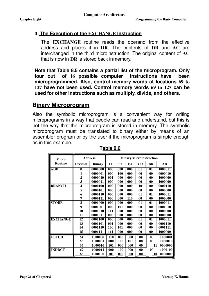
ComputerArchitecture Chapter Eight Programming the Basic Computer 4. The Execution of the EXCHANGE Instruction The EXCHANGE routine reads the operand from the effective address and places it in DR. The contents of DR and AC are interchanged in the third microinstruction. The original content of AC that is now in DR is stored back inmemory. Note that Table 8.5 contains a partial list of the microprogram. Only four out of 16 possible computer microprogrammed. Also, control memory words at locations 69 to 127 have not been used. Control memory words 69 to 127 can be used for other instructions such as multiply, divide, and others. instructions have been Binary Microprogram Also the symbolic microprogram is a convenient way for writing microprograms in a way that people can read and understand, but this is not the way that the microprogram is stored in memory. The symbolic microprogram must be translated to binary either by means of an assembler program or by the user if the microprogram is simple enough as in this example. Table 8.6 Address Binary Microinstruction Micro Routine ADD Decimal 0 1 2 3 4 5 6 7 8 9 10 11 12 13 14 15 64 65 66 67 68 Binary 0000000 0000001 0000010 0000011 0000100 0000101 0000110 0000111 0001000 0001001 0001010 0001011 0001100 0001101 0001110 0001111 1000000 1000001 1000010 1000011 1000100 F1 000 000 001 000 000 000 000 000 000 000 111 000 000 001 100 111 110 000 101 000 101 F2 000 100 000 000 000 000 000 000 000 101 000 000 000 000 101 000 000 100 000 100 000 F3 000 000 000 000 000 000 000 110 000 000 000 000 000 000 000 000 000 101 000 000 000 CD 01 00 00 00 10 00 01 00 01 00 00 00 01 00 00 00 00 00 00 00 00 BR 01 00 00 00 00 00 01 00 01 00 00 00 01 00 00 00 00 00 AD 1000011 0000010 1000000 1000000 0000110 1000000 1000011 1000000 1000011 0001010 1000000 1000000 1000011 0001110 0001111 1000000 1000001 1000010 11 0000000 1000100 10 0000000 BRANCH STORE EXCHANGE FETCH INDRCT 00 Page 21 of Chapter8 Yacoup K.Hanna
ComputerArchitecture ChapterEight Programming the Basic Computer The equivalent binary form of the microprograms is listed in Table 8.6 above. The addresses for control memory are given in both decimal and binary. The binary content of each microinstruction is derived from the symbols and their equivalent binary values as defined in Tables 8.2, 8.3, and 8.4. Notes: 1. Address 3 has no equivalent in the symbolic microprogram since the ADD routine has only three microinstructions at addresses 0, 1, and 2. The next routine starts at address4. 2. Even though address 3 is not used, some binary value must be specified for each word in control memory. We could have specified all 0's in the word since this location will never be used. However; if some unforeseen error occurs, or if a noise signal sets CAR to the value of 3, it will be wise to jump to address 64, which is the beginning of the fetch routine. 4. Design of Control Unit The microinstruction format usually is divided into fields, each field provides control bits to initiate microoperations in the system, special bits to specify the way that the next address is to be evaluated, and an address field forbranching. The method of grouping mutually exclusive variables into fields and encoding the k bits in each field to provide 2kmicrooperations is used to reduce the number of control bits that initiate microoperations. Each field requires a decoder to produce the corresponding controlsignals. This method has an advantage of reducing the size of the microinstruction bits with the following drawbacks: - 1. It requires additional hardware external to the control memory. 2. Increase the delay time of the control signals because they must propagate through the decoding circuits. Page 22 of Chapter8 Yacoup K.Hanna
ComputerArchitecture ChapterEight Programming the Basic Computer The encoding of control bits was demonstrated in the programming example of the preceding section. The nine bits of the microoperation field are divided into three subfields of three bits each. The control memory output of each subfield must be decoded to provide the distinct microoperations. The outputs of the decoders are connected to the appropriate inputs in the processorunit. Figure 8.6 shows the three 3 x 8 decoders. Each decoder is used to decode one field of the microinstruction presently available in the output of control memory to provide eight outputs. Each output of these decoders is connected to the proper circuit of the processor unit to initiate the corresponding microoperation as specified in Tables 8.2, 8.3, and 8.4. Figure 8.6 Examples 1. When Fl = 101 (binary 5), the next clock pulse transition transfers the content of DR (0-10) to AR (symbolized by DRTAR in Table 8.2). 2. When Fl = 110 (binary 6), the next clock pulse transition transfers the content of PC toAR (symbolized by PCTAR in Table 8.2). Page 23 of Chapter8 Yacoup K.Hanna
ComputerArchitecture ChapterEight Programming the Basic Computer From the examples above, it is clear that the multiplexers select information from DR when output 5 is active and from PC when output 5 is inactive. The other outputs of the decoders that initiate transfers between registers must be connected in a similarmanner. The arithmetic logic shift unit can be designed as in figures 6.20 and 21.of chapter 6. Instead of using gates to generate the control signals marked by the symbols AND, ADD, and DR in figure 6.21, inputs will now come from the outputs of the decoders associated with the symbols AND, ADD, and DRTAC, respectively, as shown in figure 8.6. these The other outputs of the decoders that are associated with an AC operation must also be connected to the arithmetic logic shift unit in a similar manner. Microprogram Sequencer The basic components of a microprogrammed control unit are: - 1. The control memory. 2. The circuits thatselect the nextaddress. The address selection part is called a Microprogram Sequencer. The purpose of the microprogram sequencer is to present an address to the control memory so that a microinstruction may be read and executed. The next-address logic of the sequencer determines the specific address source to be loaded into the control address register (CAR). The choice of the address source is guided by the next-address information bits that the sequencer receives from the presentmicroinstruction. Commercial sequencers include within the unit an internal register stack used for temporary storage of addresses during microprogram looping and subroutine calls. Some sequencers provide an output register which can function as the address register for the control memory. Page 24 of Chapter8 Yacoup K.Hanna
ComputerArchitecture ChapterEight Programming the Basic Computer To illustrate the internal structure of a typical microprogram sequencer, we will show a particular unit that is suitable for use in the microprogram computer example developed in the precedingsection. Figure 8.7 shows the block diagram of the microprogram sequencer. The control memory is included in the diagram to show the interaction between the sequencer and the memory attached toit. Figure 8.7 1. There are two multiplexers in the circuit. a. The first multiplexer symbolized by MUX1 selects an address from one of four sources and transfer it into a control address register CAR. The output from CAR provides the address for a given word in the control memory. b. The second multiplexer symbolized by MUX2 tests the value of selected status bit and the result of the test is applied to an input logic circuits. Page 25 of Chapter8 Yacoup K.Hanna
ComputerArchitecture Chapter Eight Programming the Basic Computer The four inputs to MUX1 come from:- The incremented content of CAR which is applied to one of the multiplexer inputs and to the subroutine register(SBR). The address field of the presentmicroinstruction. The outputs ofSBR. The external source that maps theinstruction. 2. The diagram shows a single subroutine register. a typical sequencer will have a register stack about four to eight levels deep. In this way, a number of subroutines can be active at the same time. A push and pop operation, in conjunction with a stack pointer, stores and retrieves the return address during the call and returnmicroinstructions. 3. The input logic circuit. The condition field (CD) of the microinstruction selects one of the status bits in the second multiplexer (MUX1). If the bit selected is equal to 1, the T (test) variable is equal to 1; otherwise, it is equal to 0. The T value together with the two bits from the branch field (BR) goes to an input logiccircuit. The input logic in a particular sequencer will determine the type of operations that are available in the unit. Typical sequencer operations are: increment, branch or jump, call and return from subroutine, load an external address, push or pop the stack, and other address sequencing operations. With three inputs, the sequencer can provide up to eight address sequencing operations. Some commercial sequencers have three or four inputs in addition to the T input and thus provide a wider range of operations. The input logic circuit in figure 8.7 has three inputs, I0, I1, and T, and three outputs, S0, S1, and L. Variables S0 and S1 select one of the source addresses for CAR. Variable L enables the load input in SBR. The binary values of the two selection variables determine the path in the multiplexer. For example, with S1S0= 10, multiplexer input number 2 is selected and establishes a transfer path from SBR to CAR. Note that each of the four inputs as well as the output of MUX 1 contains a 7-bit address. Page 26 of Chapter8 Yacoup K.Hanna
ComputerArchitecture Chapter Eight Programming the Basic Computer Table 8.7 shows the truth table for the input logic circuit. Inputs I1 and I0 are identical to the bit values in the BR field. The function listed in each entry was defined in Table 8.3. The bit values for S1 and S0 are determined from the stated function and the path in the multiplexer that establishes the required transfer. The subroutine register is loaded with the incremented value of CAR during a call microinstruction (BR = 01) provided that the status bit condition is satisfied (T = 1). Table 8.7 Input I1 I0 T 0 0 0 0 0 1 0 1 1 0 1 1 MUX1 S1 0 0 0 0 1 1 BR Field 0 0 0 0 0 1 0 1 1 0 1 1 LoadSBR L 0 0 0 1 0 0 S0 0 1 0 1 0 1 0 1 0 1 x x The truth table can be used to obtain the simplified Boolean functions for the input logic circuit: S1 = I1 S0 = I1 I0 + I1T L = I1 I0T The circuit can be constructed with three AND gates, an OR gate, and an inverter. Page 27 of Chapter8 Yacoup K.Hanna
ComputerArchitecture ChapterEight Programming the Basic Computer Note that the incrementer circuit in the sequencer of figure 8.7 is not a counter constructed with flip-flops but rather a combinational circuit constructed with gates. A combinational circuit incrementer can be designed by cascading a series of half-adder circuits as shown in figure 8.8. The output carry from one stage must be applied to the input of the next stage. One input in the first least significant stage must be equal to 1 to provide the increment-by-one operation. Figure 8.8 Page 28 of Chapter8 Yacoup K.Hanna
ComputerArchitecture ChapterEight Programming the Basic Computer Problems 1. Define the following: (a) Microoperation. (b) Microinstruction. (c) Microprogram. (d) Microcode. 2. The microprogrammed control organization shown in Figure 8.1 has the fol- lowing propagation delay times. 40 ns to generate the next address, 10 ns to transfer the address into the control address register, 40 ns to access the control memory ROM, 10 ns to transfer the microinstruction into the control data register, and 40 ns to perform the required microoperations specified by the control word. What is the maximum clock frequency that the control can use? What would the clock frequency be if the control data register is not used? The control memory in figure 8.2 has 4096 words of 24 bitseach. 3. a. How many bits are there in the control address register? b. How many bits are there in each of the four inputs shown going into the multiplexers? c. What are the number of inputs in each multiplexer and how many multiplexers are needed? 4. Using the mapping procedure described in figure 8.3, give the first microinstructionaddress forthefollowingoperationcode: (a) 0010. (b) 1011. (c) 1111. 5. Formulate a mapping procedure that provides 8 consecutive microinstructions for each routine. The operation code has six bits and the control memory has 2048 words. 6. Explain how the mapping from an instruction code to a microinstruction address can be done by means of a read-only memory. What is the advantage of this method compared to the one in figure 8.3? Page 29 of Chapter8 Yacoup K.Hanna
ComputerArchitecture ChapterEight Programming the Basic Computer 8.7. Using Table 8.2, give the 9-bit microoperation field for the following microoperations: a. AC AC + 1, b. PC PC +1, c. DR AC, DR DR + 1 DR M[AR] AC DR 8. Using Table 8.2, convert the following symbolic microoperations to register transfer statements and to binary. a. READ, INCPC b. ACTDR, DRTAC c. ARTPC, DRTAC, WRITE Suppose that we change the ADD routine listed in Table 8.5 to the following two microinstructions. ADD: READ I CALL INDR2 9. FETCH ADD U JMP What should be subroutine INDR2? 8.10. The following is a symbolic microprogram for an instruction in the computer defined in section 8.3. ORG40 NOP S JMP FETCH NOP Z JMP FETCH NOP I CALL INDRCT ARTPC U JMP FETCH a. Specify the operation performed when the instruction is executed. b. Convert the four microinstructions into their equivalent binary form. 8.11. Add the following instructions to the computer of Section 8.3 (EA is the effective address). Write the symbolic microprogram for each routine as in Table 8.5. (Note that AC must not change in value unless the instruction specifies a change in AC). Page 30 of Chapter8 Yacoup K.Hanna
ComputerArchitecture ChapterEight Programming the Basic Computer Symbol Opcode AND SUB ADM BTCL BZ SEQ BPNZ Symbolic Function AC AC M [EA] AC AC M [EA] M [EA] M [EA] + AC AC AC M [EA] If (AC = 0) then (PC EA) If (AC = M [EA] ) then (PC PC + 1) If (AC > 0) then (PC EA) Description 0100 0101 0110 0111 1000 1001 1010 AND Subtract Add to memory Bit clear Branch if AC zero Skip if equal Branch if positive and nonzero 12. Show how outputs 5 and 6 of decoder F3 in figure 8.6 are to be connected to the program counterPC. Show how a 9-bit microoperation field in a microinstruction can be divided into subfields to specify 46 microoperations. How many microoperations can be specified in onemicroinstruction? 13. A computer has 16 registers, an ALU (arithmetic logic unit) with 32 operations, and a shifter with eight operations, all connected to a common bus system. a. Formulate a control word for a microoperation. b. Specify the number of bits in each field of the control word and give a general encoding scheme, c. Show the bits of the control word that specify the microoperation. 14. 15. Assume that the input logic of the microprogram sequencer of figure 8.7 has four inputs, I2, I1, I0, T (test), and three outputs, S1, S0, and L. The operations that are performed in the unit are listed in the following table. Design the input logic circuit using a minimum number of gates. I2 I1 I0 0 0 x 0 0 1 0 1 1 0 1 1 1 Operation Increment CAR if T = 1, jump to AD if T = 0 Jump to ADunconditionally Increment CAR unconditionally Jump to AD if T = 1, incrementCAR if T = 0 Callsubroutineif T = 1, increment CARif T = 0 Return from subroutineunconditionally Map external addressunconditionally 0 1 0 0 0 1 1 1 Page 31 of Chapter8 Yacoup K.Hanna