Reduced Voltage Operation in Modern DRAM Devices Experimental Characterization

DRAM power is crucial in modern systems, and reducing voltage can enhance efficiency. Explore the impact on reliability, latency, and energy with new mechanisms like Voltron. Address high power consumption, low-voltage memory designs, and goals like understanding DRAM characteristics and developing energy reduction mechanisms. Key questions focus on voltage effects on reliability and latency, along with designing energy-saving mechanisms.

Download Presentation

Please find below an Image/Link to download the presentation.
The content on the website is provided AS IS for your information and personal use only. It may not be sold, licensed, or shared on other websites without obtaining consent from the author.If you encounter any issues during the download, it is possible that the publisher has removed the file from their server.
You are allowed to download the files provided on this website for personal or commercial use, subject to the condition that they are used lawfully. All files are the property of their respective owners.
The content on the website is provided AS IS for your information and personal use only. It may not be sold, licensed, or shared on other websites without obtaining consent from the author.
E N D
Presentation Transcript
Understanding Reduced-Voltage Operation in Modern DRAM Devices Experimental Characterization, Analysis, and Mechanisms Kevin Chang A. Giray Yaglikci , Saugata Ghose , Aditya Agrawal*, Niladrish Chatterjee*, Abhijith Kashyap , Donghyuk Lee*, Mike O Connor*, Hasan Hassan , Onur Mutlu *
Executive Summary DRAM (memory) power is significant in today s systems Existing low-voltage DRAM reduces voltage conservatively Goal: Understand and exploit the reliability and latency behavior of real DRAM chips under aggressive reduced-voltage operation Key experimental observations: Errors occur and increase with lower voltage Errors exhibit spatial locality Higher operation latency mitigates voltage-induced errors Voltron: A new DRAM energy reduction mechanism Reduce DRAM voltage without introducing errors Use a regression model to select voltage that does not degrade performance beyond a chosen target 7.3% system energy reduction 2
Outline Executive Summary Motivation DRAM Background Characterization of DRAM Voltron: DRAM Energy Reduction Mechanism Conclusion 3
High DRAM Power Consumption Problem: High DRAM (memory) power in today s systems >40% in POWER7 (Ware+, HPCA 10) >40% in GPU (Paul+, ISCA 15) 4
Low-Voltage Memory Existing DRAM designs to help reduce DRAM power by lowering supply voltage conservatively ????? ???????2 DDR3L (low-voltage) reduces voltage from 1.5V to 1.35V (-10%) LPDDR4 (low-power) employs low-power I/O interface with 1.2V (lower bandwidth) Can we reduce DRAM power and energy by furtherreducing supply voltage? 5
Goals 1 Understand and characterize the various characteristics of DRAM under reduced voltage 2 Develop a mechanism that reduces DRAM energy by lowering voltage while keeping performance loss within a target 6
Key Questions How does reducing voltage affect reliability(errors)? How does reducing voltage affect DRAMlatency? How do we design a new DRAM energy reduction mechanism? 7
Outline Executive Summary Motivation DRAM Background Characterization of DRAM Voltron: DRAM Energy Reduction Mechanism Conclusion 8
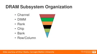
High-Level DRAM Organization DRAM chips DRAM Channel DRAM Module 9
DRAM Chip Internals DRAM Cell Bitline DRAM Array Peripheral Circuitry Wordline Control Logic Bank S S S S I/O Sense amplifiers (row buffer) Off-chip channel 10
DRAM Operations 1 ACTIVATE: Store the row into the row buffer 1 1 1 1 2 READ: Select the target cache line and drive to CPU 3 PRECHARGE: Prepare the array for a new ACTIVATE to I/O 11
DRAM Access Latency 1 Activation latency (13ns / 50 cycles) 2 Precharge latency (13ns / 50 cycles) ACTIVATE READ PRECHARGE Command 1 1 1 1 Cache line (64B) Data Duration Next ACT 12
Outline Executive Summary Motivation DRAM Background Characterization of DRAM Experimental methodology Impact of voltage on reliability and latency Voltron: DRAM Energy Reduction Mechanism Conclusion 13
Supply Voltage Control on DRAM DRAM Module Supply Voltage Adjust the supply voltage to every chip on the same module 14
Custom Testing Platform SoftMC [Hassan+, HPCA 17]: FPGA testing platform to 1) Adjust supply voltage to DRAM modules 2) Schedule DRAM commands to DRAM modules Existing systems: DRAM commands not exposed to users DRAM module Voltage controller FPGA https://github.com/CMU-SAFARI/DRAM-Voltage-Study https://github.com/CMU-SAFARI/DRAM-Voltage-Study 15
Tested DRAM Modules 124DDR3L (low-voltage) DRAM chips 31 SO-DIMMs 1.35V (DDR3 uses 1.5V) Density: 4Gb per chip Three major vendors/manufacturers Manufacturing dates: 2014-2016 Iteratively read every bit in each 4Gb chip under a wide range of supply voltage levels: 1.35V to 1.0V (-26%) 16
Outline Executive Summary Motivation DRAM Background Characterization of DRAM Experimental methodology Impact of voltage on reliability and latency Voltron: DRAM Energy Reduction Mechanism Conclusion 17
Reliability Worsens with Lower Voltage Errors induced by reduced-voltage operation Min. voltage (Vmin) without errors Nominal Voltage Reducing voltage below Vmin causes an increasing number of errors 18
Source of Errors Detailed circuit simulations (SPICE) of a DRAM cell array to model the behavior of DRAM operations https://github.com/CMU-SAFARI/DRAM-Voltage-Study https://github.com/CMU-SAFARI/DRAM-Voltage-Study 20 Activate Precharge Latency (ns) Nominal Voltage 15 Circuit model 10 5 0.9 1.0 Supply Voltage (V) 1.1 1.2 1.3 Reliable low-voltage operation requires higher latency 19
DIMMs Operating at Higher Latency Measured minimum latency that does not cause errors in DRAM modules 40% of modules Activate Latency (ns) Measured Minimum 14 Distribution of latency in the total population 100% of modules 12 10 8 DRAM requires longer latency to access data Lower bound of latency as our latency adjustment granularity is 2.5ns without errors at lower voltage 20
Spatial Locality of Errors A module under 1.175V (12% voltage reduction) Errors concentrate in certain regions 21
Other Results in the Paper Error-Correcting Codes (ECC) ECC (SECDED) is not sufficient to mitigate the errors Effect of temperature Higher temperature requires higher latency under some voltage levels Data retention time Lower voltage does not require more frequent refreshes Effect of stored data pattern on error rate Difference is not statistically significant to draw conclusion 22
Summary of Key Experimental Observations Voltage-induced errors increase as voltage reduces further below Vmin Errors exhibit spatial locality Increasing the latency of DRAM operations mitigates voltage-induced errors 23
Outline Executive Summary Motivation DRAM Background Characterization of DRAM Experimental methodology Impact of voltage on reliability and latency Voltron: DRAM Energy Reduction Mechanism Conclusion 24
DRAM Voltage Adjustment to Reduce Energy Goal: Exploit the trade-off between voltage and latency to reduce energy consumption Approach: Reduce DRAM voltage reliably Performance loss due to increased latency at lower voltage Performance High Power Savings Bad Performance DRAM Power Savings Low Power Savings Good Performance Nominal Voltage (%) Improvement Over 40 30 20 10 0 -10 -20 0.9 1.0 1.1 1.2 1.3 Supply Voltage (V) 25
Voltron Overview Voltron User specifies the performance loss target Select the minimum DRAM voltage without violating the target How do we predict performance loss due to increased latency under low DRAM voltage? 26
Linear Model to Predict Performance Voltron User specifies the performance loss target Select the minimum DRAM voltage without violating the target Application s characteristics Min. Voltage Final Voltage [ [- -1%, 1%, - -3%, Predicted performance loss 3%, ] ] [1.3V, 1.25V, [1.3V, 1.25V, ] ] DRAM Voltage Target Linear regression model 27
Linear Model to Predict Performance Application s characteristics for the model: Memory intensity: Frequency of last-level cache misses Memory stall time: Amount of time memory requests stall commit inside CPU Handling multiple applications: Predict a performance loss for each application Select the minimum voltage that satisfies the performance target for all applications 28
Comparison to Prior Work Prior work: Dynamically scale frequency and voltage of the entire DRAM based on bandwidth demand[David+, ICAC 11] Problem: Lowering voltage on the peripheral circuitry decreases channel frequency (memory data throughput) Voltron: Reduce voltage to only DRAM array without changing the voltage to peripheral circuitry DRAM Array Peripheral Circuitry DRAM Array Peripheral Circuitry Control Logic Control Logic Low Low Voltage Bank Voltage Bank I/O I/O Prior Work Voltron Off-chip channel High frequency Off-chip channel Low frequency 29
Exploiting Spatial Locality of Errors Key idea: Increase the latency only for DRAM banks that observe errors under low voltage Benefit: Higher performance Peripheral Circuitry DRAM Array Control Logic Bank 0 Bank 1 Bank 2 I/O Off-chip channel High latency Low latency 30
Outline Executive Summary Motivation DRAM Background Characterization of DRAM Experimental methodology Impact of voltage on reliability and latency Voltron: DRAM Energy Reduction Mechanism Evaluation Conclusion 31
Voltron Evaluation Methodology Cycle-level simulator: Ramulator [CAL 15] McPAT and DRAMPower for energy measurement https://github.com/CMU-SAFARI/ramulator https://github.com/CMU-SAFARI/ramulator 4-core system with DDR3L memory Benchmarks: SPEC2006, YCSB Comparison to prior work: MemDVFS[David+, ICAC 11] Dynamic DRAM frequency and voltage scaling Scaling based on the memory bandwidth consumption 32
Energy Savings with Bounded Performance MemDVFS [David+, ICAC 11] Voltron Meets performance target 0 8 7.3% Performance Loss (%) 7 -1 More savings for high bandwidth applications Energy Savings (%) 6 CPU+DRAM -2 -1.6% -1.8% 5 -3 4 3.2% 3 -4 2 1. Voltron improves energy for both low and high intensity workloads -5 1 Performance Target -6 0 Low High 2. Voltron satisfies the performance loss target via a regression model Low Memory Intensity High Memory Intensity 33
Outline Executive Summary Motivation DRAM Background Characterization of DRAM Experimental methodology Impact of voltage on reliability and latency Voltron: DRAM Energy Reduction Mechanism Conclusion 34
Conclusion DRAM (memory) power is significant in today s systems Existing low-voltage DRAM reduces voltage conservatively Goal: Understand and exploit the reliability and latency behavior of real DRAM chips under aggressive reduced-voltage operation Key experimental observations: Errors occur and increase with lower voltage Errors exhibit spatial locality Higher operation latency mitigates voltage-induced errors Voltron: A new DRAM energy reduction mechanism Reduce DRAM voltage without introducing errors Use a regression model to select voltage that does not degrade performance beyond a chosen target 7.3% system energy reduction 35
Understanding Reduced-Voltage Operation in Modern DRAM Devices Experimental Characterization, Analysis, and Mechanisms Kevin Chang A. Giray Yaglikci , Saugata Ghose , Aditya Agrawal*, Niladrish Chatterjee*, Abhijith Kashyap , Donghyuk Lee*, Mike O Connor*, Hasan Hassan , Onur Mutlu *
BACKUP 37
Derivation of More Precise Latency Circuit-level SPICE simulation Potential latency range DRAM circuit model validates our experimental results and provides more precise latency 42
Performance Loss Correlation Observation: Application s performance loss due to higher latency has a strong linear relationship with its memory intensity Degradation (%) Voltage = 1.1V (-23%) DRAM Latency +13% Voltage = 1.2V (-13%) DRAM Latency +5% Performance Memory Intensity (MPKI) Memory Intensity (MPKI) MPKI = Last-level cache Misses Per Thousand Instruction 43
Performance-Aware Voltage Adjustment Build a performance (linear-regression) model to predict performance loss based on the selected voltage ????????????? = ?0+ ?1??????? + ?2???.???????? + ?3???.????????? Latency due to voltage adjustment The running application s characteristics ?s are trained through 151 application samples Use the model to select a minimum voltage that satisfies a performance loss target specified by the user 44
Linear Model Accuracy R2 = 0.75 / 0.9 for low and high intensity workloads RMSE = 2.8 / 2.5 for low and high intensity workloads 45