Resistor Transistor Logic (RTL) vs. Diode Transistor Logic (DTL): A Comparison
Explore the characteristics, operations, and circuit diagrams of Resistor Transistor Logic (RTL) and Diode Transistor Logic (DTL) families. Learn about their key differences, fan-out, noise immunity, power dissipation, propagation delay, and noise margin to understand their applications in digital circuits.

Download Presentation

Please find below an Image/Link to download the presentation.
The content on the website is provided AS IS for your information and personal use only. It may not be sold, licensed, or shared on other websites without obtaining consent from the author. If you encounter any issues during the download, it is possible that the publisher has removed the file from their server.
You are allowed to download the files provided on this website for personal or commercial use, subject to the condition that they are used lawfully. All files are the property of their respective owners.
The content on the website is provided AS IS for your information and personal use only. It may not be sold, licensed, or shared on other websites without obtaining consent from the author.
E N D
Presentation Transcript
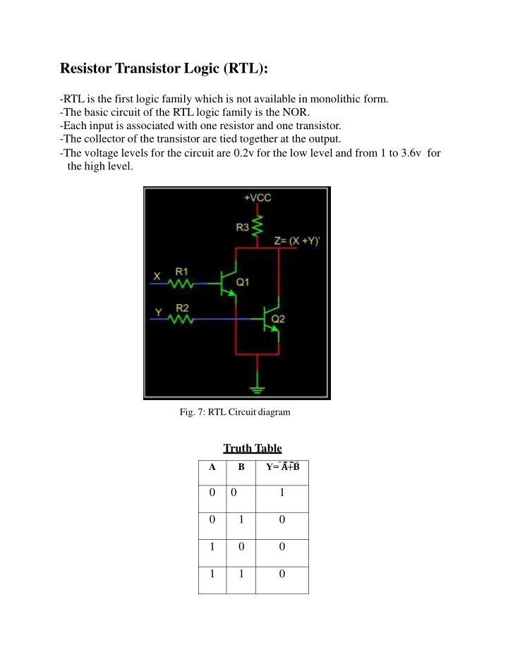
Resistor Transistor Logic (RTL): -RTL is the first logic family which is not available in monolithic form. -The basic circuit of the RTL logic family is the NOR. -Each input is associated with one resistor and one transistor. -The collector of the transistor are tied together at the output. -The voltage levels for the circuit are 0.2v for the low level and from 1 to 3.6v for the high level. Fig. 7: RTL Circuitdiagram Truth Table A B Y= ? + ? 0 0 1 0 1 0 1 0 0 1 1 0
136 Operation: If any input is high: The corresponding transistor is driven into saturation and the output goes low, regardless of the states of the other transistor. If all inputs are low: Then all transistor are in cutoff state and the output of the circuit goes high. Characteristics : It has a fan-out of 5. Propagation delay is 25 ns. Power dissipation is 12 mw. Noise margin for low signal input is 0.4 v. Poor noise immunity. Low speed. Diode Transistor Logic (DTL): - DTL was first commercial available IC logic family in 53/73 series. - The basic circuit in the DTL logic is the NAND gate. - Each input associated with one diode. -The diode and resistor form an AND gate. -The transistor services as a NOR gate.
Fig.8: DTL Circuit diagram 137 Truth Table A B Y= ? . ? 0 0 1 0 1 1 1 0 1 1 1 0 Operation: If any input is low: The corresponding diode conducts current through Vcc and resistor into the input node. The voltage at point p is equal to the input voltage + diode drop. This is an insufficient voltage for conduction of a transistor. Since the voltage at point p is 0v then the transistor is cut off state and the output is logic 1. If all inputs are high: The transistor is driven into saturation region. The voltage at point p is high. Hence the output is low.
Characteristics : It has fan-out of 8. It has high noiseimmunity. Power dissipation is 12mw. Propagation delay is average 30ns. Noise margin is about 0.7V.
:")