SEM Instrument: Construction, Operation, and Applications
Learn about the scanning electron microscope (SEM) instrument, its construction, high resolution imaging capabilities, and applications for characterizing nanomaterials. Discover how SEM works, its components like the electron gun and vacuum system, and the importance of interaction volume in producing detailed images. Explore the imaging techniques of SEM, such as secondary electrons and backscattered electrons, to understand surface morphology and composition analysis.

Download Presentation

Please find below an Image/Link to download the presentation.
The content on the website is provided AS IS for your information and personal use only. It may not be sold, licensed, or shared on other websites without obtaining consent from the author. If you encounter any issues during the download, it is possible that the publisher has removed the file from their server.
You are allowed to download the files provided on this website for personal or commercial use, subject to the condition that they are used lawfully. All files are the property of their respective owners.
The content on the website is provided AS IS for your information and personal use only. It may not be sold, licensed, or shared on other websites without obtaining consent from the author.
E N D
Presentation Transcript
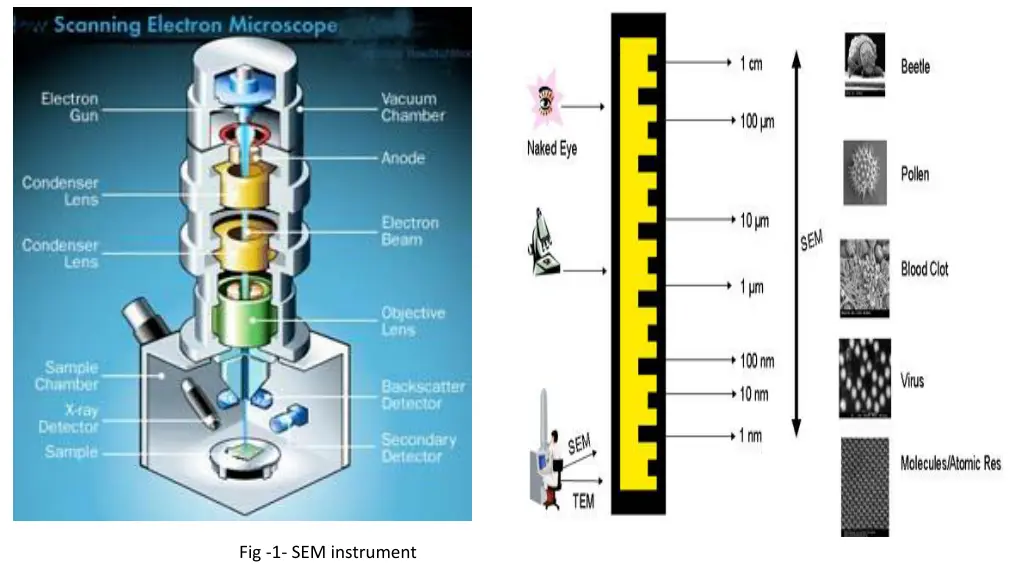
Scanning electron microscope SEM SEM is one of the most widely techniques used in characterization of nanomaterails. The resolution of SEM approaches a few nanimaterials ( 10 nm). The instrument can easily operates magnification up to 500,000 times which is higher than optical microscope (2000 times). SEM provide topographical surface information, morphology, and chemical composition of materials. In typical SEM, an electron beam with very fine size ( 10 nm) and having energy from few hundreds up to 50 Kev that is scanned over the sample surface by deflection coils. As electron strike and penetrate the surface, a number of interaction occur and resulting in emission of electrons and photons. SEM images are produced by collecting the emitted electrons on a cathode ray tube. SEM samples can be either bulk or powder. The specimen is mounted on carbon tape and must be dried. The specimen is most be conductive to prevent charging. Non-conductive specimens are coated with a thin film of conductive materials such as gold by ion sputtering method. Figure -2- a) carbon tabe, b) sample stage
Construction of SEM 1. Electron Gun To have high resolution, field emission electron gun is preferred. In this type of emission, high electric field applied to the metal (tungsten wire welded to tungsten tip with a curvature radius of 100 nm) and electrons are emitted from the tungsten. Beam diameter about 10 nm as contrast to thermionic gun ( 10 to 20 m) 2. Anode A metal plate which has a positive charge. It attracts the electrons to form a beam. 3.Lenses Placing a lens below electron gun to adjust the diameter of electron beam. Condenser lens (magnetic lens) uses to control the diameter of the beam and beam current depending on the lens strength. Objective lens use to focus the electron beam into the sample. 4. Scanning coil Consists of two rolls of wires face each other to move the beam backwards and forwards across the surface. 5. Vacuum system The inside of the SEM must be clean from any contamination, so it is kept under high vacuum ( 10-3 10-8 pa). Inert gas such as nitrogen pumped inside the SEM. 6. Sample stage The stage is used to hold the samples and can be moved in (x,y,z) direction, also can be rotated.
Interaction Volume When the accelerated beam electrons strike a specimen they penetrate inside it to depths of about 1-3 m and interact both elastically and inelastically with the solid, forming a limiting interaction volume from which various types of radiation emerge, including BSE, SE, x-rays, and cathodoluminescence in some materials. The resulting region over which the incident electrons interact with the sample is known as interaction volume. The interaction volume has several important characteristics, which determine the nature of imaging in the SEM.
For secondary electrons resulting from inelastic interaction where incident electron ( primary electron) loss some of its energy to the orbital electron of sample and the electron will emit from the sample called ( secondary electron). Secondary electrons emitting depth is from 10 to 100 nm and uses to give the surface topography. Its energy about 50 ev Backscattered electrons are elastically scattered with no loss energy where incident electron interact with atom nucleus. BSE are emitted from much larger depths compared to SE and has high energy as incident electron energy. BSE is useful for contrast between different regions. Regions of high average atomic number will appear bright relative to regions of low atomic number. Ultimately the resolution in the SEM is controlled by the size of the interaction volume. Secondary electron Backscattered electrons
Figure-4- Backscattered image of Al-Cu composite ( al atomic number is 13, Cu atomic number is 29) Figure -3- Secondary electron image of Gold nanoparticles with size of 10 nm Figure -5- Backscattered and secondary electrons image of Ti-Si ( Ti atomic number is 24 and Si atomic number is 12
Energy dispersion x-ray ( EDX) resulting as incident electron strike unexcited atoms, electrons from inner shell will be ejected and leave a hole. Electrons from higher shell will fill the hole and release excess energy as x-ray which is used EDX or ejecting the third electeon known as Auger electron. Since each atom in periodic table has a unique electronic structure with a unique set of energy levels, both x-ray emission and Auger are used to determine chemical compositions of the sample. Table of x-ray emission for some elements.
Defect in SEM imaging : Charging As explained before, the incident electrons are entered to the specimen and loss their energy when the specimen is conductive. If specimen is not conductive, the incident electrons will accumulate at the surface ( that is charging ), and number of electrons exit from the specimen is less than electrons hit the specimen. Charging causes the SEM image appears in in broken way. Figure -7- charging effect on SEM images
Charging could be prevented by : 1. Coating with a thin film of conductive metals ( Au, Pt ) 1. Low accelerating voltage: The number of secondary electrons increased as the accelerating voltage is decreased. This means, the number of SE electrons are equal to the number of incident electrons at low accelerating voltage. So, even the non-conductive materials such as ceramic can be imaged without charging. Fig -8- Compare between high voltage mode and low voltage mode of insulator materials


 resulting as incident")
 resulting as incident")