Six-Step Voltage Source Inverter Characteristics
"Discover the characteristics of a Six-Step Voltage Source Inverter, its unique waveforms, gating signals, line-to-line voltages, and harmonic frequency components. Learn about the absence of certain harmonics in this efficient inverter design."

Download Presentation

Please find below an Image/Link to download the presentation.
The content on the website is provided AS IS for your information and personal use only. It may not be sold, licensed, or shared on other websites without obtaining consent from the author. If you encounter any issues during the download, it is possible that the publisher has removed the file from their server.
You are allowed to download the files provided on this website for personal or commercial use, subject to the condition that they are used lawfully. All files are the property of their respective owners.
The content on the website is provided AS IS for your information and personal use only. It may not be sold, licensed, or shared on other websites without obtaining consent from the author.
E N D
Presentation Transcript
ELGC06 3-phase Inverters 1
ORGANIZATION I. Voltage Source Inverter (VSI) A. Six-Step VSI B. Pulse-Width Modulated VSI II. PWM Methods A. Sine PWM B. Hysteresis (Bang-bang) C. Space Vector PWM III. References 2
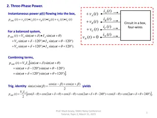
I. Voltage Source Inverter (VSI) A. Six-Step VSI (1) Six-Step three-phase Voltage Source Inverter Fig. 1 Three-phase voltage source inverter. 3
I. Voltage Source Inverter (VSI) A. Six-Step VSI (2) Gating signals, switching sequence and line to negative voltages Fig. 2 Waveforms of gating signals, switching sequence, line to negative voltages for six-step voltage source inverter. 4
I. Voltage Source Inverter (VSI) A. Six-Step VSI (3) Switching Sequence: 561 (V1) 612 (V2) 123 (V3) 234 (V4) 345 (V5) 456 (V6) 561 (V1) where, 561 means that S5, S6 and S1 are switched on Fig. 3 Six inverter voltage vectors for six-step voltage source inverter. 5
I. Voltage Source Inverter (VSI) A. Six-Step VSI (4) Line to line voltages (Vab, Vbc, Vca) and line to neutral voltages (Van, Vbn, Vcn) Line to line voltages Vab = VaN - VbN Vbc = VbN - VcN Vca = VcN - VaN Phase voltages Van = 2/3VaN - 1/3VbN - 1/3VcN Vbn = -1/3VaN + 2/3VbN - 1/3VcN Vcn = -1/3VaN - 1/3VbN + 2/3VcN Fig. 4 Waveforms of line to neutral (phase) voltages and line to line voltages for six-step voltage source inverter. 6
I. Voltage Source Inverter (VSI) A. Six-Step VSI (5) Amplitude of line to line voltages (Vab, Vbc, Vca) Fundamental Frequency Component (Vab)1 3 4 V 6 dc 2 = = (V ) (rms) V . 0 78 V ab 1 dc dc 2 Harmonic Frequency Components (Vab)h : amplitudes of harmonics decrease inversely proportional to their harmonic order . 0 78 h = (V ) (rms) V h ab dc = = where, h 6n 1 (n 1, 2, 3,.....) 7
I. Voltage Source Inverter (VSI) A. Six-Step VSI (6) Characteristics of Six-step VSI It is called six-step inverter because of the presence of six steps in the line to neutral (phase) voltage waveform Harmonics of order three and multiples of three are absent from both the line to line and the line to neutral voltages and consequently absent from the currents Output amplitude in a three-phase inverter can be controlled by only change of DC-link voltage (Vdc) 8
I. Voltage Source Inverter (VSI) B. Pulse-Width Modulated VSI (1) Objective of PWM Control of inverter output voltage Reduction of harmonics Disadvantages of PWM Increase of switching losses due to high PWM frequency Reduction of available voltage EMI problems due to high-order harmonics 9
I. Voltage Source Inverter (VSI) B. Pulse-Width Modulated VSI (2) Pulse-Width Modulation (PWM) Fig. 5 Pulse-width modulation. 10
I. Voltage Source Inverter (VSI) B. Pulse-Width Modulated VSI (3) Inverter output voltage When vcontrol > vtri, VA0 = Vdc/2 When vcontrol < vtri, VA0 = -Vdc/2 Control of inverter output voltage PWM frequency is the same as the frequency of vtri Amplitude is controlled by the peak value of vcontrol Fundamental frequency is controlled by the frequency of vcontrol Modulation Index (m) ( ) v peak of V 0 1 control v A = = , m / 2 V tri dc where, (V ) : fundamenta l frequecny 11 component of V A0 1 A0
II. PWM METHODS A. Sine PWM (1) Three-phase inverter Fig. 6 Three-phase Sine PWM inverter. 12
II. PWM METHODS A. Sine PWM (2) Three-phase sine PWM waveforms vcontrol_C vcontrol_ B vtri vcontrol_A Frequency of vtri and vcontrol Frequency of vtri = fs VA 0 Frequency of vcontrol = f1 where, fs = PWM frequency f1 = Fundamental frequency VB0 VC0 Inverter output voltage VA B When vcontrol > vtri, VA0 = Vdc/2 VBC When vcontrol < vtri, VA0 = -Vdc/2 where, VAB = VA0 VB0 VBC = VB0 VC0 VCA = VC0 VA0 VCA t Fig. 7 Waveforms of three-phase sine PWM inverter. 13
II. PWM METHODS A. Sine PWM (3) Amplitude modulation ratio (ma) ( 0 1 ), peak amplitude amplitude of control v peak value V of V = = A m a / 2 of v tri dc where, (V ) : fundamental frequecny component of V A0 1 3 , U 2 A0 U 2 = = U m 0,95U 2, U the rms line voltage value (phase or phase to phase) i ab1,rms a i i,rms i,rms Frequency modulation ratio (mf) where, , 1 f mf should be an odd integer f s = = = f PWM frequency and f fundamenta l frequency m s 1 f if mf is not an integer, there may exist subhamonics at output voltage if mf is not odd, DC component may exist and even harmonics are present at output voltage mf should be a multiple of 3 for three-phase PWM inverter An odd multiple of 3 and even harmonics are suppressed 14
II. PWM METHODS B. Hysteresis (Bang-bang) PWM (1) Three-phase inverter for hysteresis Current Control Fig. 8 Three-phase inverter for hysteresis current control. 15
II. PWM METHODS B. Hysteresis (Bang-bang) PWM (2) Hysteresis Current Controller Fig. 9 Hysteresis current controller at Phase a . 16
II. PWM METHODS B. Hysteresis (Bang-bang) PWM (3) Characteristics of hysteresis Current Control Advantages Excellent dynamic response Low cost and easy implementation Drawbacks Large current ripple in steady-state Variation of switching frequency No intercommunication between each hysteresis controller of three phases and hence no strategy to generate zero-voltage vectors. As a result, the switching frequency increases at lower modulation index and the signal will leave the hysteresis band whenever the zero vector is turned on. The modulation process generates subharmonic components 17


")
")
")
")
")
")
")
")
")