Small-Signal Method for Component Variations in Non-linear Networks
Calculate the effect of parameters change in non-linear networks using small-signal analysis. Explore how variations impact the DC solution of a network when components undergo small changes. Examples include resistance changes and MOSFET behavior in nominal and actual states. Understand the approximate solutions through small-signal circuit analysis.

Download Presentation

Please find below an Image/Link to download the presentation.
The content on the website is provided AS IS for your information and personal use only. It may not be sold, licensed, or shared on other websites without obtaining consent from the author. If you encounter any issues during the download, it is possible that the publisher has removed the file from their server.
You are allowed to download the files provided on this website for personal or commercial use, subject to the condition that they are used lawfully. All files are the property of their respective owners.
The content on the website is provided AS IS for your information and personal use only. It may not be sold, licensed, or shared on other websites without obtaining consent from the author.
E N D
Presentation Transcript
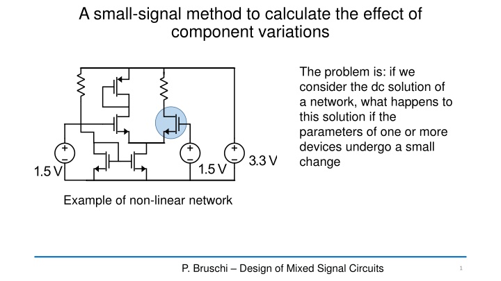
A small-signal method to calculate the effect of component variations The problem is: if we consider the dc solution of a network, what happens to this solution if the parameters of one or more devices undergo a small change Example of non-linear network P. Bruschi Design of Mixed Signal Circuits 1
Small signal approach to parameter variations parameter (P) Network Sub-Network (N) ( ( ) ) ( ( ) ) = = = = , , I I g V V g V V , , , , I I f V V P f V V P 1 1 1 2 1 1 1 2 Two port net. (Q) N: Q: 2 2 1 2 2 2 1 2 We consider that the component whose parameters change can be represented by a two-port network Both the selected two-port network (Q) and the remaining network (N) can be highly non-linear (g1,g2,f1,f2: non-linear) + P P P Variation of the network solution P. Bruschi Microelectronic System Design 2
Approximate solution based on small signal analysis Apply two-currents to the nominal network, as in the figure, with values: N I P I P = = 1P i P 2P i P 1 2 The variations caused by the change P-> P+ P can be calculated solving the small-signal circuit of the whole network with the only independent sources i1Pand i2P. 1P i 2P i P. Bruschi Microelectronic System Design 3
Example of parameter change: resistance change I P = 1P i P 1 I1 I2 R V1 V2 R R i1P I P = = 0 i P 2 2 P + R R R 1 V R R R R R V R I R = = = I = R 1 2 R Vth 1P i R 1 1 = I R = V i R 1 1 th P P. Bruschi Microelectronic System Design 4
MOSFET = = = 0 I I I I 1 G I P I P g = = 0 i P 1 P 2 D = = V V V V = 1 GS i P D 2 p 2 DS : , P V t I I V = + i V D D 2 p t t P. Bruschi Microelectronic System Design 5
MOSFET: strong inversion + saturation actual device nominal device nominal device 2p i , V V nominal parameters + V + , V t t t , , V I nominal operating point GS DS D ( ) 2 I V V D GS t 2 1 2 I I V ( ) ( ) 2 = = + V V V V V i V D D GS t GS t t 2 p t t P. Bruschi Microelectronic System Design 6
MOSFET: strong inversion + saturation 1 2 ( ) ( ) 2 = i V V V V V 2 p GS t GS t t 2 ( ) 2 ( ) 2 V V V V V ( ) GS t t 2 V V GS t 2 GS t 2 V D I DEF = = D I t V i I ( ) 2 p D V GS t P. Bruschi Microelectronic System Design 7
Matched devices Quantity of interest 1. The two device are nominally identical. 2. The nominal bias conditions (quiescent currents and voltages) are identical. 3. The nominal transfer functions that tie the quantity of the interest for the circuit (for example the output voltage of an amplifier) to the parametric currents of the two devices ( ID1 and ID2) are opposite. ( ) = F I = U F I I 1,2 1 2 D D D P. Bruschi Microelectronic System Design 8
Matched devices = + P P P 1 1 N 1P i I P I P ( ) = = U F i i F P P M1 1 2 1 2 P P F = + U P P P -F 2 2 N Same functions, calculated at the same operating point because the device are matched 2P i M2 I P I P ( ) ( ) = = U F P P F P P P P 1 2 1 2 N N I P ( ) ( ) DEF = U F P P = P P P 1 2 1 2 1,2 P. Bruschi Microelectronic System Design 9
Matched Mosfets Combined effect of two matched MOSFETs ( ) = = F I U F I I 1 2 1,2 D D D = 2 V 2 , 1 V 2 1 ) 2 , 1 t 2 , 1 = I I ( = V V 2 , 1 D D V V 2 , 1 t 2 1 t t GS t Effect of parameter change of a single device: , 2 V 1,2 1 2 F I = t V I ( ) D D , V V V V GS t 1,2 2 1 t t t P. Bruschi Microelectronic System Design 10
Norton equivalent circuit with dc component Probing a non.linear network with an arbitrary voltage source V Test 1. Short circuit current when the probing source assumes a voltage VB. (complete solution, including dc components) P. Bruschi Microelectronic System Design 11
Norton equivalent circuit with dc component V = B R out I SC Note: Rout is the small-signal resistance seen across terminals H-K in the operating point forced by imposing voltage VBacross H-K terminals P. Bruschi Microelectronic System Design 12
Equivalent circuit of the network The equivalent circuit is valid until voltage VHKis close enough to VBthat the output resistance does not change significantly P. Bruschi Microelectronic System Design 13
Example: equivalent circuit of the output termination of a real amplifier 2: Rout 1: ISC possible choice: V V = Vdd dd B 2 M2 Vout = I I I 2 1 SC D D ( ) = , ..., , ...... I f V V i nk i V M1 = // R r r 1 2, 1 SC in in n dd 1 2 out d d P. Bruschi Microelectronic System Design 14