Solar Cell Surface Design Principles
Anti-reflection coatings and surface texturing are crucial aspects of solar cell design to minimize reflection and enhance light trapping efficiency. By utilizing ellipsometry or visual inspection, the thickness of anti-reflection coatings can be accurately determined. Surface texturing techniques, such as random pyramid and inverted pyramid texturing, alter the crystalline structure to optimize light absorption. Light trapping mechanisms increase the optical path length within the cell, promoting better energy conversion. Enhancing the understanding of these design principles can lead to more efficient solar cell technology.

Download Presentation

Please find below an Image/Link to download the presentation.
The content on the website is provided AS IS for your information and personal use only. It may not be sold, licensed, or shared on other websites without obtaining consent from the author.If you encounter any issues during the download, it is possible that the publisher has removed the file from their server.
You are allowed to download the files provided on this website for personal or commercial use, subject to the condition that they are used lawfully. All files are the property of their respective owners.
The content on the website is provided AS IS for your information and personal use only. It may not be sold, licensed, or shared on other websites without obtaining consent from the author.
E N D
Presentation Transcript
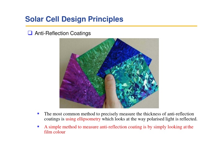
Solar Cell Design Principles Anti-Reflection Coatings The most common method to precisely measure the thickness of anti-reflection coatings is using ellipsometry which looks at the way polarised light is reflected. A simple method to measure anti-reflection coating is by simply looking atthe film colour
Solar Cell Design Principles Surface Texturing Surface texturing, either in combination with an anti-reflection coating or by itself, can also be used to minimise reflection. Any "roughening" of the surface reduces reflection by increasing the chances of reflected light bouncing back onto the surface, rather than out to the surrounding air.
Solar Cell Design Principles Surface Texturing The crystalline structure of silicon results in a surface made up of pyramids if the surface is appropriately aligned with respect to the internal atoms. This type of texturing is called "random pyramid" texture[2], and is commonly used in industry for single crystalline wafers.
Solar Cell Design Principles Surface Texturing Another type of surface texturing used is known as "inverted pyramid" texturing. Using this texturing scheme, the pyramids are etched down into the silicon surface rather than etched pointing upwards from the surface.
Solar Cell Design Principles LightTrapping The optimum device thickness is not controlled solely by the need to absorb all the light. For example, if the light is not absorbed within a diffusion length of the junction, then the light-generated carriers are lost to recombination. Consequently, an optimum solar cell structure will typically have "light trapping" in which the optical path length is several times the actual device thickness, where the optical path length of a device refers to the distance that an unabsorbed photon may travel within the device before it escapes out of the device. This is usually defined in terms of device thickness. For example, a solar cell with no light trapping features may have an optical path length of one device thickness, while a solar cell with good light trapping may have an optical path length of 50, indicating that light bounces back and forth within the cell many times. Light trapping is usually achieved by changing the angle at which light travels in the solar cell by having it be incident on an angled surface. A textured surfacewill not only reduce reflection as previously described but will also couple light obliquely into the silicon, thus giving a longer optical path length than the physical device thickness.
Solar Cell Design Principles Light Trapping In a textured single crystalline solar cell, the presence of crystallographic planes make the angle 1 equal to 36 as shownbelow.
Solar Cell Design Principles Light Trapping Using total internal reflection, light can be trapped inside the cell and make multiple passes through the cell, thus allowing even a thin solar cell to maintain a high optical path length.
Solar Cell Design Principles Lambertian Rear Reflectors Using total internal reflection, light can be trapped inside the cell and make multiple passes through the cell, thus allowing even a thin solar cell to maintain a high optical path length. High reflection off the rear cell surface reduces absorption in the rear cell contacts or transmission from the rear, allowing the light to bounce back into the cell for possible absorption.
Solar Cell Design Principles Recombination Losses Recombination losses effect both the current collection (and therefore the short- circuit current) as well as the forward bias injection current (and therefore the open-circuit voltage). Recombination is frequently classified according to the region of the cell in which it occurs. Typically, recombination at the surface (surface recombination) or in the bulk of the solar cell (bulk recombination) are the main areas of recombination. The depletion region is another area in which recombination can occur (depletion region recombination).
Solar Cell Design Principles Current Losses Due to Recombination In order for the p-n junction to be able to collect all of the light-generated carriers, both surface and bulk recombination must be minimised. In silicon solar cells, the two conditions commonly required for such current collection are: 1. the carrier must be generated within a diffusion length of the junction, so that it will be able to diffuse to the junction before recombining; and 2. in the case of a localised high recombination site (such as at an unpassivated surface or at a grain boundary in multicrystalline devices), the carrier must be generated closer to the junction than to the recombination site. For less severe localised recombination sites, (such as a passivated surface), carriers can be generated closer to the recombination site while still being able to diffuse to the junction and be collected without recombining. The presence of localised recombination sites at both the front and the rear surfaces of a silicon solar cell means that photons of different energy will have different collection probabilities.
Solar Cell Design Principles Current Losses Due to Recombination Since blue light has a high absorption coefficient and is absorbed very close to the front surface, it is not likely to generate minority carriers that can be collected by the junction if the front surface is a site of high recombination. Similarly, a high rear surface recombination will primarily affect carriers generated by infrared light, which can generate carriers deep in the device. The quantum efficiency of a solar cell quantifies the effect of recombination on the light generation current. The quantum efficiency of a silicon solar cell is shown below.
Solar Cell Design Principles Voltage Losses Due to Recombination The open-circuit voltage is the voltage at which the forward bias diffusion current is exactly equal to the short circuit current. The forward bias diffusion current is dependent on the amount recombination in a p-n junction and increasing the recombination increases the forward bias current. Consequently, high recombination increases the forward bias diffusion current, which in turn reduces the open-circuit voltage. The material parameter which gives the recombination in forward bias is the diode saturation current. The recombination is controlled by the number of minority carriers at the junction edge, how fast they move away from the junction and how quickly they recombine. Consequently, the dark forward bias current, an hence the open-circuit voltage is affected by the following parameters:
Solar Cell Design Principles Voltage Losses Due to Recombination 1. the number of minority carriers at the junction edge. The number of minority carriers injected from the other side is simply the number of minority carriers in equilibrium multiplied by an exponential factor which depends on the voltage and the temperature. Therefore, minimising the equilibrium minority carrier concentration reduces recombination. Minimising the equilibrium carrier concentration is achieved by increasing the doping; 2. the diffusion length in the material. A low diffusion length means that minority carriers disappear from the junction edge quickly due to recombination, thus allowing more carriers to cross and increasing the forward bias current. Consequently, to minimise recombination and achieve a high voltage, a high diffusion length is required. The diffusion length depends on the types of material, the processing history of the wafer and the doping in the wafer. High doping reduces the diffusion length, thus introducing a trade-off between maintaining a high diffusion length (which affects both the current and voltage) and achieving a high voltage; 3. the presence of localised recombination sources within a diffusion length of the junction. A high recombination source close the the junction (usually a surface or a grain boundary) will allow carriers to move to this recombination source very quickly and recombine, thus dramatically increasing the recombination current. The impact of surface recombination is reduced by passivating the surfaces.
Solar Cell Design Principles Voltage Losses Due to Recombination
Solar Cell Design Principles Surface Recombination Surface recombination can have a major impact both on the short-circuit current and on the open-circuit voltage. High recombination rates at the top surface have a particularly detrimental impact on the short-circuit current since top surface also corresponds to the highest generation region of carriers in the solar cell. Lowering the high top surface recombination is typically accomplished by reducing the number of dangling silicon bonds at the top surface by using "passivating" layer on the top surface. The majority of the electronics industry relies on the use of a thermally grown silicon dioxide layer to passivate the surface due to the low defect states at the interface.
Solar Cell Design Principles Surface Recombination Since the passivating layer for silicon solar cells is usually an insulator, any region which has an ohmic metal contact cannot be passivated using silicon dioxide. Instead, under the top contacts the effect of the surface recombination can be minimised by increasing the doping. While typically such a high doping severely degrades the diffusion length, the contact regions do not participate in carrier generation and hence the impact on carrier collection is unimportant.
Solar Cell Design Principles Back Surface Field A similar effect is employed at the rear surface to minimise the impact of rear surface recombination velocity on voltage and current if the rear surface is closer than a diffusion length to the junction. A "back surface field" (BSF) consists of a higher doped region at the rear surface of the solar cell. The interface between the high and low doped region behaves like a p-n junction and an electric field forms at the interface which introduces a barrier to minority carrier flow to the rear surface. The minority carrier concentration is thus maintained at higher levels in the bulk of the device and the BSF has a net effect of passivating the rear surface.
Top Contact Design Series Resistance In addition to maximising absorption and minimising recombination, the final condition necessary to design a high efficiency solar cell is to minimise parasitic resistive losses. Both shunt and series resistance losses decrease the fill factor and efficiency of a solar cell. A detrimentally low shunt resistance is a processing defect rather than a design parameter. However, the series resistance, controlled by the top contact design and emitter resistance, needs to be carefully designed for each type and size of solar cell structure in order to optimise solar cell efficiency.
Top Contact Design Series Resistance The metallic top contacts are necessary to collect the current generated by a solar cell. "Busbars" are connected directly to the external leads, while "fingers" are finer areas of metalization which collect current for delivery to the busbars. The key design trade-off in top contact design is the balance between the increased resistive losses associated with a widely spaced grid and the increased reflection caused by a high fraction of metal coverage of the top surface.
Solar Cell Structure Silicon Solar Cell Parameters For silicon solar cells, the basic design constraints on surface reflection, carrier collection, recombination and parasitic resistances result in an optimum device of about 25% theoretical efficiency.
Solar Cell Structure Basic Cell Design SubstrateMaterial In particular, silicon's band gap is slightly too low for an optimum solar cell and since silicon is an indirect material, it has a low absorption co-efficient. While the low absorption co-efficient can be overcome by light trapping, silicon is also difficult to grow into thin sheets. However, silicon's abundance, and its domination of the semiconductor manufacturing industry has made it difficult for other materials to compete. Cell Thickness (100-500 m) An optimum silicon solar cell with light trapping and very good surface passivation is about 100 m thick. However, thickness between 200 and 500 m are typically used, partly for practical issues such as making and handling thin wafers, and partly for surface passivation reasons.
Solar Cell Structure Basic Cell Design Doping of Base (1 cm) A higher base doping leads to a higher Vocand lower resistance, but higher levels of doping result in damage to the crystal Reflection Control (front surface typically textured) The front surface is textured to increase the amount of light coupled into the cell. Emitter Dopant (n-type) N-type silicon has a higher surface quality than p-type silicon so it is placed at the front of the cell where most of the light is absorbed. Thus the top of the cell is the negative terminal and the rear of the cell is the positive terminal.
Solar Cell Structure Basic Cell Design Emitter Thickness (<1 m) A large fraction of light is absorbed close to the front surface. By making the front layer very thin, a large fraction of the carriers generated by the incoming light are created within a diffusion length of the p-n junction. Doping Level of Emitter (100 / ) The front junction is doped to a level sufficient to conduct away the generated electricity without resistive loses. However, excessive levels of doping reduces the material's quality to the extent that carriers recombine before reaching the junction. Grid Pattern (fingers 20 to 200 m width, placed 1 - 5 mm apart) The resistivity of silicon is too low to conduct away all the current generated, so a lower resistivity metal grid is placed on the surface to conduct away the current. The metal grid shades the cell from the incoming light so there is a compromise between light collection and resistance of the metal grid.
Solar Cell Structure Basic Cell Design RearContact The rear contact is much less important than the front contact since it is much further away from the junction and does not need to be transparent. The design of the rear contact is becoming increasingly important as overall efficiency increases and the cells become thinner. Efficiency and Solar Cell Cost Under laboratory conditions and with current state-of-the-art technology, it is possible to produce single crystal silicon solar cells close to 25% efficient. However, commercially mass produced cells are typically only 13-14% efficient. The overriding reason for this difference in efficiency is that the research techniques used in the laboratory are not suitable for commercial production within the photovoltaic industry and therefore lower cost techniques, which result in lower efficiency, are used. However, it is estimated module efficiencies over 20% could be produced commercially.