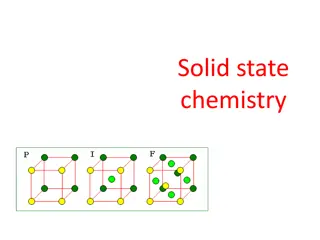
Solid State Chemistry & Catalysis
Delve into the realm of solid-state chemistry with a focus on materials chemistry and catalysis in Lecture 3 of the course taught by Rob Jackson. Explore key concepts and applications in this fascinating field to broaden your understanding. Contact Rob Jackson at r.a.jackson@keele.ac.uk for more information.

Download Presentation

Please find below an Image/Link to download the presentation.
The content on the website is provided AS IS for your information and personal use only. It may not be sold, licensed, or shared on other websites without obtaining consent from the author.If you encounter any issues during the download, it is possible that the publisher has removed the file from their server.
You are allowed to download the files provided on this website for personal or commercial use, subject to the condition that they are used lawfully. All files are the property of their respective owners.
The content on the website is provided AS IS for your information and personal use only. It may not be sold, licensed, or shared on other websites without obtaining consent from the author.
E N D
Presentation Transcript
CHE-30043 Materials Chemistry & Catalysis : Solid State Chemistry lecture 3 Rob Jackson LJ1.16, 01782 733042 r.a.jackson@keele.ac.uk www.facebook.com/robjteaching @robajackson
Lecture plan Compound semiconductors III/V and II/VI compounds Band gaps and the appearance of materials Determination of conductivity measurements Band structures of d block compounds band gaps from che-30043 lecture 3 2
Compound semiconductors Compound semiconductors are compounds that show semiconductor behaviour (in contrast to the insulating compounds earlier). A commercially important example is GaAs, gallium arsenide. GaAs has a similar structure to Si (the diamond structure) with alternating Ga and As atoms. considered http://phycomp.technion.ac.il/~nika/diamond_structure.html che-30043 lecture 3 3
GaAs First, look at the valence electrons: Ga is 4s24p1, As is 4s24p3 There will be 2 bands formed, each with 4N levels (the band structure will be drawn). The lower band will have a greater contribution from As than Ga (nuclear charge higher in As). The 8N valence electrons fill the lower band. The band gap is ~ 1.4 eV. che-30043 lecture 3 4
Other III/V semiconductors GaAs is an example of a III/V semiconductor (a combination of an element from group 3, with one valence electron less than Si, with one from group V, with one valence electron more than Si). Other examples are GaSb, InP, InAs and InSb. che-30043 lecture 3 5
II/VI semiconductors II/VI semiconductors are typified by CdTe. Cd has valence electrons in 5s24d10 Te has valence electrons in 5s24d105p4 Band structure is based on 5s and 5p levels from each element. The band structure of CdTe will be drawn as an example. Other examples include ZnTe and ZnS. che-30043 lecture 3 6
Compound semiconductors: trend in band gaps Band gap 300K, eV 2.25 Band gap 300K, eV 3.2 material material GaP ZnO* GaAs GaSb InP InAs InSb 1.43 0.68 1.27 0.36 0.17 ZnS* CdSe CdTe Si Ge 3.6 1.74 1.44 1.11 0.66 * Note wide band gaps Kittel, C., Intro. to Solid State Physics, 6th Ed., New York: John Wiley, 1986, p. 185 che-30043 lecture 3 7
Applications of semiconductors: photocells (i) A good example of the use of semiconductors is in photocells. Photocells work because electricity is conducted and a circuit completed when light shines on a semiconducting material but thus will only work if the bandgap is in the visible region. che-30043 lecture 3 8
Applications of semiconductors: photocells (ii) What values of bandgaps are useful? Use E = hc/ e.g., for a cell to be useful in the visible region, the bandgap must be low enough for the lowest wavelength) light. Red light has =700 nm = 700 x 10-9 m Calculate E and convert to eV frequency (longest che-30043 lecture 3 9
Band gaps and colour/appearance of materials - 1 Absorption/reflection of light by metals and compounds depends structure/band gap, since the photons that are absorbed and then re-emitted will have appropriate frequencies for the band gaps of the materials in question. on their band che-30043 lecture 3 10
Band gaps and colour/appearance of materials - 2 Metals transitions between levels in bands correspond to visible appearance. Silicon band gap in lower end of visible region shiny metallic appearance. Insulators (e.g. crystalline NaCl, SiO2) larger band gaps higher energy corresponding, e.g. to UV region colourless but changed by defects ... light shiny che-30043 lecture 3 11
Decreasing band gap and colour Germanium described as grey-white C (diamond) clear and transparent Silicon showing shiny appearance (but not transparent) che-30043 lecture 3 12
Relationship between band structure and crystal structure in group IV C Si Ge Sn Pb band gap/eV 5.5 1.1 0.7 0.1 0.1 che-30043 lecture 3 13
Crystal structure - 1 In C, Si and Ge the valence s and p orbitals can combine hence the sp3 model is a valid description and all valence electrons go into bonding orbitals and fill the valence band. In Sn and Pb there is less overlap of the s and p orbitals so separate bonding and antibonding orbitals are not formed. che-30043 lecture 3 14
Crystal structure - 2 Instead the orbitals form a continuous band, with a very small band gap, as in metallic structures. In general, the structure that is formed is the one which involves the electrons most in bonding, and this is achieved differently in metals, through having delocalised valence electrons. che-30043 lecture 3 15
Why the band gap decreases going down the C group The degree of s, p overlap decreases as nuclear charge increases (going down the group). At Sn there is virtually no overlap, and a continuous band is formed from the s and p orbitals. As the degree of overlap decreases, both the bond strength, and the difference between bonding and antibonding orbitals decreases. che-30043 lecture 3 16
Determination of band gaps from conductivity measurements An insulator or semiconductor will show an increase in conductance (the inverse of resistance) with temperature. Conductance G is related to temperature T by the expression: G = G0 exp (-Eg / 2kT) where Eg is the band gap of the material. che-30043 lecture 3 17
Determination of Eg from data T/K 300 G 0.1 350 0.5 400 3.0 Procedure is to take the expression and take logs of both sides: ln G = ln G0 Eg / 2kT Plot ln G against 1/T, gradient = - Eg / 2k A rough plot will be drawn in the lecture. che-30043 lecture 3 18
Band structures of d block compounds We consider the first row transition metal monoxides: MO, where M = Ti, V, Mn, Fe, Co and Ni Structures are based on the rock salt structure, but their properties differ widely because of the behaviour of the d-orbitals, which control their properties. che-30043 lecture 3 19
MO Structure revisited All the MO compounds adopt this structure, but their properties vary widely che-30043 lecture 3 20
Classification of d-orbitals The metal d-orbitals are divided into two sets, one pointing towards the oxide ions and one between them. The two sets of orbitals will be drawn, and are also shown on the next slide (or see Dann pp 111-3) The t2g orbitals on each metal atom (dxy, dyz, dzx) point towards other metal atoms, and the other d orbitals overlap with orbitals from the oxygen atoms. che-30043 lecture 3 21
Classification of d-orbitals http://chimge.unil.ch/En/lc/1LC20.htm che-30043 lecture 3 22
Can bands form? If the metal t2g d-orbitals can overlap, then bands can form. Also, these bands will not be fully occupied because the d-orbitals are themselves not filled. So, if bands can form, the oxides will have metallic properties and be conductors. This applies to TiO and VO. che-30043 lecture 3 23
Trends in properties along the group With TiO and VO there is good overlap of the d orbitals, so they have metallic properties and conduct electricity. As we move along the group, the d-orbital electrons become more tightly bound (with increasing nuclear charge) and this inhibits band formation. The oxides show semiconductor and then insulator properties. che-30043 lecture 3 24
TiO VO MnO FeO CoO NiO metals semiconductors insulators Colour of the compounds can also be a useful indication of their conductivity. Nickel oxide is green, as is a nickel complex in solution, suggesting discrete nickel ions with well-spaced energy levels. Vanadium oxide is black light is absorbed over the full spectral range, corresponding to many closely spaced energy levels. che-30043 lecture 3 25
Summary Compound described The influence of band gaps on the appearance of materials has been considered The determination of band gaps from conductivity measurements described The band structures of d block compounds has been described semiconductors have been has been che-30043 lecture 3 26