Explore the world of complex oxide perovskite semiconductors and the application of computational methods like Hartree-Fock and Density Functional Theory in understanding electronic materials. Learn about Vienna Ab-initio Simulation Package and comparisons of band structures using GGA and HSE. Dive into the exciting realm of materials research in this detailed scientific discourse.
Please find below an Image/Link to download the presentation.
The content on the website is provided AS IS for your information and personal use only. It may not be sold, licensed, or shared on other websites without obtaining consent from the author. If you encounter any issues during the download, it is possible that the publisher has removed the file from their server.
You are allowed to download the files provided on this website for personal or commercial use, subject to the condition that they are used lawfully. All files are the property of their respective owners.
The content on the website is provided AS IS for your information and personal use only. It may not be sold, licensed, or shared on other websites without obtaining consent from the author.
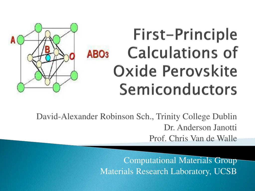
Complex Oxide Perovskite Semiconductors; Crystals of the form ABO3 A = Mono-, Di- or Trivalent element; Li, K, Mg, Ca, Sr, Ba, Sc, Y, La, Gd B = Transition Metal cation; Ti, Zr, Hf, Y, Nb, Ta or; Al, Ga, In SrTiO3 Valence band maximum Implications? Explaining experimental results using fundamental theory. Novel electronic materials. Transparent conductors; Wide Band-Gap Semiconductors. 2
We wish to solve the many-electron quantum mechanical equations for the electronic structure of solids. Hartree-Fock (HF) The many-electron wavefuntion is written as an anti-symmetric linear combination of single electron wavefunctions. Density Functional Theory (DFT) Replaces the many-electron problem with a single-particle in an effective potential. 1998 Nobel Prize awarded to Walter Kohn for his work on DFT. Hybrid Functionals Heyd-Scuseria-Ernzerhof (HSE) Mixes both HF and DFT exchange potential to give a more accurate description of the electronic structure. 3
Vienna Ab-initio Simulation Package (VASP) code A self-consistent iterative method which works to minimise the energy of the system by filling up electron bands and relaxing the lattice constant in turn Solves the quantum mechanical Schr dinger equation. The calculation uses First Principle methods and so no empirical input parameters are needed. High Performance Computing California NanoSystems Institute (CNSI), UCSB. Lattice, Guild and Knot clusters. Lonestar Cluster, Texas Advanced Computing Center, U Texas. Computer Programming Linux, bash, VI, XMGrace 4
SrHfO3 Band Structure Plot Comparisons using GGA (General Gradient Approximation) SrTiO3 a = 0.4142 nm ; Eg = 3.70 eV SrZrO3 a = 0.3948 nm ; Eg = 1.65 eV a = 0.4194 nm ; Eg = 3.18 eV 5
SrHfO3 Band Structure Plot Comparisons using HSE (Heyd-Scuseria-Ernzerhof ) SrTiO3 a = 0.4109 nm ; Eg = 5.30 eV SrZrO3 a = 0.3905 nm ; Eg = 3.33 eV a = 0.4142 nm ; Eg = 4.88 eV 6
HSE vs. GGA Accepted experimental values a = 0.3905 nm; Eg = 3.25 eV SrTiO3 using GGA SrTiO3 using HSE a = 0.3948 nm; Eg = 1.65 eV a = 0.3905 nm ; Eg = 3.33 eV 7
Lattice Constants and Indirect R- band gaps, using GGA and HSE On using HSE we get band gap widening of 1.54 0.16 eV Crystal a (nm) [GGA] [HSE] a (nm) Eg (eV) [GGA] Eg (eV) [HSE] Eg diff (eV) BaTiO3 BaZrO3 CaTiO3 GdAlO3 GdGaO3 LaAlO3 LaGaO3 MgTiO3 ScAlO3 SrTiO3 SrZrO3 YAlO3 0.4038 0.4251 0.3896 0.3726 0.3843 0.3810 0.3928 0.3851 0.3646 0.3948 0.4194 0.3718 0.3993 0.4228 0.3851 0.3684 0.3796 0.3777 0.3874 0.3800 0.3606 0.3905 0.4142 0.3681 1.54 2.99 1.70 2.90 2.81 3.49 3.34 1.60 1.42 1.65 3.18 2.80 3.18 4.51 3.41 4.33 4.23 4.89 4.75 3.18 2.86 3.33 4.88 4.36 1.64 1.51 1.71 1.43 1.42 1.39 1.41 1.58 1.44 1.69 1.70 1.56 8
Band Alignment Calculations; Gives a Valence Band Offset of 0.44 eV LaAlO3-SrTiO3 Electrostatic Potential, V Displacement, x 9
The Valence Band Offset is given by where VBMi is the Valance Band Maximum of material i, and is the Averaged Electrostatic Potential in the bulk region of an interface calculation. SrTiO3 SrZrO3 0.98 eV Conduction Band Eg = 4.88 eV Eg = 3.33 eV Valence Band 0.57 eV 10
The electronic bandstructure of cubic perovskites were determined from first principles. The valence bands of oxide perovskite are composed mostly of oxygen p-states. The conduction bands are determined by the B-cation orbitals. The use of hybrid functionals increase the band gaps by 1.54 0.16 eV. Most of the band offsets are determined by the conduction bands. 11
My supervisor Dr. Anderson Janotti and faculty advisor Prof. Chris Van de Walle Daniel Steiauf, John Lyons, Cyrus Dreyer, Luke Gordon and all the other members of the Van de Walle Computational Materials Group. The School of Physics, The University of Dublin, Trinity College and the SFI. 12


 code")