Strategies for Emittance Reduction in Solid Photocathodes
Explore limits and strategies for reducing emittance in solid photocathodes due to surface non-uniformities like physical roughness, quantum scale effects, and chemical roughness. Discover techniques involving disordered and ordered surfaces to optimize electron emission efficiency.

Uploaded on | 0 Views
Download Presentation

Please find below an Image/Link to download the presentation.
The content on the website is provided AS IS for your information and personal use only. It may not be sold, licensed, or shared on other websites without obtaining consent from the author. If you encounter any issues during the download, it is possible that the publisher has removed the file from their server.
You are allowed to download the files provided on this website for personal or commercial use, subject to the condition that they are used lawfully. All files are the property of their respective owners.
The content on the website is provided AS IS for your information and personal use only. It may not be sold, licensed, or shared on other websites without obtaining consent from the author.
E N D
Presentation Transcript
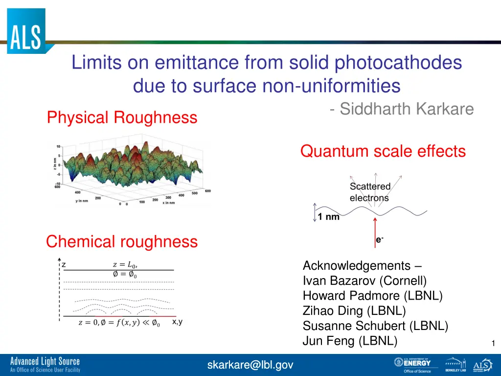
Limits on emittance from solid photocathodes due to surface non-uniformities - Siddharth Karkare Physical Roughness Quantum scale effects Chemical roughness Acknowledgements Ivan Bazarov (Cornell) Howard Padmore (LBNL) Zihao Ding (LBNL) Susanne Schubert (LBNL) Jun Feng (LBNL) 1 skarkare@lbl.gov skarkare@lbl.gov
Where we are? ??? (???/??) MTE =1 ??? ?? MTE ??2 2 2? ? = 1 eV (1.4 m/mm) Practically used in most photoinjectors 100 meV (0.44 m/mm) 25-40 meV near threshold Metals Very low QE<10-7 Alkali-antimonides Low QE <10-4. GaAs/(Cs,O) Very long response time 10 meV (0.14 m/mm) ULTRACOLD ELECTRONS 1 meV (0.04 m/mm) 2 skarkare@lbl.gov
Strategies to reduce emittance Disordered surfaces Disordered over layers on ordered materials (GaAs(Cs/O)) Polycrystalline/amorphous materials (alkali antimonides, polished metals) Emission best explained by 3-step model Dowell s theory for polycrystalline metals and alkali antimonides Monte-Carlo simulations for GaAs(Cs/O) Both assume isotropic emission of electrons ??? ??????? ?? if ??????? 0 Strategy: Operate at near threshold and cryo-cool cathodes Physical and chemical roughness both will be an issue 3 skarkare@lbl.gov
Strategies to reduce emittance Ordered surfaces Can obtain LEED pattern, Clean auger spectrum Have not been demonstrated in guns so far Emittance given by band-structure Use low transverse effective mass Surface states Hole-like bands Physical roughness by definition not an issue for most ordered materials Chemical roughness may be present due to varying surface terminations 4 skarkare@lbl.gov
Limits on emittance from solid photocathodes due to surface non-uniformities - Siddharth Karkare Physical Roughness Quantum scale effects Chemical roughness 5 skarkare@lbl.gov skarkare@lbl.gov
Physical roughness First discussed by Bradley Slope effect and Field Effect D.J. Bradley et al., J. Phys. D: Appl. Phys 10, 111 (1977) For disordered surfaces isotropic emission near 0 K.E at emission Negligible slope effect Consider only field effect 6 skarkare@lbl.gov
Field effect Calculate electron trajectories in roughness distorted field to obtain increase in MTE 2? ? = 10 nm, ? = 100 nm ? MTE?????=?2?2?? for? ? 2? MTE = MTE??+ MTE????? 7 skarkare@lbl.gov
Modelling field effect Possible to calculate this for any surface by decomposing the field into Fourier components ? ????(?,?) ? = ??0+ ???? 1= 2+ ??? 2 ?? ??? Distortions due to surface roughness >> Accelerating field MTE?????=??2 2??/??? 2 ??? 2?0 ? = ??????,? ???,? = cos ???? + ??? cos(???? + ???) T. Gorlov, Journal of Electrostatics 65, 735 (2007) S. Karkare et al., Proceedings of 2011 Particle Accelerator Conference, New York, NY, USA, THP192 8 skarkare@lbl.gov
Alkali antimonide example UHV-AFM measurements Electric field 5 MV/m 20 MV/m 100 MV/m Sequential deposition 2.5 nm rms Rough cathode (sequential deposition) 16.6 meV 66.6 meV 333 meV Smooth cathode (Co- deposition) 2.1 meV 8.3 meV 41.5 meV Co-deposition 0.6 nm rms ~ 25K ~ 100K For ultra-cold electrons (~2 meV) Need atomically smooth cathodes!! 9 skarkare@lbl.gov
Limits on emittance from solid photocathodes due surface non-uniformities - Siddharth Karkare Physical Roughness Chemical roughness Quantum scale effects 10 skarkare@lbl.gov skarkare@lbl.gov
Chemical roughness surface adsorbates different grain orientations different surface terminations Kelvin Probe Force Microscopy on CsKSb Energy Resolved or Tunable wavelength PEEM Surface potential (V) ~0.5 V variations on clean polished Cu Measured at LBNL +Renault et al. Surf. Interface Anal. 2006; 38: 375 377 11 skarkare@lbl.gov
Modelling chemical roughness effect Electric field ?0= ?0 ? ?,? = ? ??? z ? = ?0, = 0 0 2? ?? sin 2? ?? is potential variation ? is periodicity x,y ? = 0, = ? ?,? 0 Say = 0.1 V, ? = 100 nm ? = 8 MV/m MTE??= 17 meV @ ?0= 10MV/m = 8 meV @ ?0= 20MV/m 2? ?? sin 2? ?? ?,?,? = ??0+ ? ??sin ?2 2? ? ?0 and ? ? ? =2? 2 MTE??= 4 2??0 ? Karkare and Bazarov, Phys. Rev Applied, 4, 024015 (2015) 12 skarkare@lbl.gov
Complications in modelling 2? ?? sin 2? ?? ?,?,? = ??0+ ? ??sin For ? ?0 - Emitted electrons can re-enter the cathode Electron emission is also non-uniform Low work function regions emit more electrons Increased space charge effects Can result in electric fields inside cathode surfaces More complications if physical and chemical roughness are present Karkare et al. Phys. Rev Applied, 4, 024015(2015) 13 skarkare@lbl.gov
Limits on emittance from solid photocathodes due surface non-uniformities - Siddharth Karkare Physical Roughness Chemical roughness Quantum scale effects 14 skarkare@lbl.gov skarkare@lbl.gov
Quantum scale effects 100 meV electrons Wavelength > 4 nm 10 meV electrons Wavelength > 10 nm For surface variations with period of few nm quantum interference matters Scattered electrons 1 nm For example Sub-nm scale surface roughness can act as a diffraction grating to scatter emitted electrons e- 15 skarkare@lbl.gov
GaAs example Simplified surface no Cs barrier, no work function variation ? ?,? = ??(?,?) ??????????= ? ?,? = cos(??) ?2 ?1 ? ?,? ? ? = 0.5 V ? 0 zmin zmax GaAs Vacuum Interface ? = ?? GaAs Vacuum ? = 0 1 nm H = 2 1 ?? + ? ? ? + ? ?,? ?(?) S(z) is the heavy-side function 2? Karkare and Bazarov, Phys. Rev Applied, 4, 024015 (2015) 16 skarkare@lbl.gov
GaAs example Scattered electrons 1 nm Sub-nm scale roughness can be due to surface reconstructions, atomic steps or surface defects Can explain experimental results Karkare and Bazarov, Phys. Rev Applied, 4, 024015 (2015) 17 skarkare@lbl.gov
Conclusions To achieve 1-2 meV scale MTE need atomically smooth cathodes Chemical roughness or work function variations can be a major obstacle Need to measure chemical roughness on cathode surfaces and develop simulations to calculate its effects on electron emission Understand quantum scale effects in photoemission 18 skarkare@lbl.gov