Understanding Combinational Circuits: Multiplexers, Decoders, ALU
Explore the implementation of multiplexers, decoders, and ALU in digital circuits, along with their use cases and logic circuits. Learn about the functionalities and structures of these essential components in digital design. Dive into circuit delays, sequential circuits, and more in this informative lecture.

Download Presentation

Please find below an Image/Link to download the presentation.
The content on the website is provided AS IS for your information and personal use only. It may not be sold, licensed, or shared on other websites without obtaining consent from the author. If you encounter any issues during the download, it is possible that the publisher has removed the file from their server.
You are allowed to download the files provided on this website for personal or commercial use, subject to the condition that they are used lawfully. All files are the property of their respective owners.
The content on the website is provided AS IS for your information and personal use only. It may not be sold, licensed, or shared on other websites without obtaining consent from the author.
E N D
Presentation Transcript
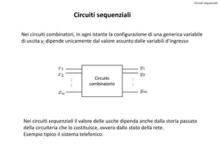
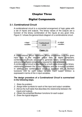
5. COMBINATIONAL CIRCUITS Rocky K. C. Chang 17 October 2017
GOALS OF THIS LECTURE Understand how multiplexers, decoders, and demultiplexers, which are basic building blocks for digital circuits are implemented. Understand how different arithmetic and logic functions are implemented in an ALU. Understand the circuit delay and its relation to sequential circuit. 2
MULTIPLEXER: USE CASE Update the PC either from PC + 4 or PC + 4 + immediate 3
MULTIPLEXER: LOGIC CIRCUIT Component Symbol Implementation Truth Table + + + A B D BD A A B D ABD 0 1 2 3 4
DECODER: USE CASE A decoderis a combinational circuit with a number of output lines, only one of which is asserted at any time. For example, it can be used to implement the write port for a register file. 5
DECODER: LOGIC CIRCUIT In general, a decoder has n inputs and 2noutputs. For a 2-to-4 decoder: = D A A 0 1 0 A0 0 0 1 1 A1 0 1 0 1 D0 1 0 0 0 D1 0 1 0 0 D2 0 0 1 0 D3 0 0 0 1 D0 D1 D2 D3 = 2-to-4 D A A A0 1 1 0 A1 Decoder = D A A 2 1 0 = D A A 3 1 0 6
For a 3-to-8 decoder 7
DEMULTIPLEXER With an additional input line, a decoder can be used as a demultiplexer. The demultiplexer connects a single input to one of several outputs. The n inputs act as an address to select a particular output line. The value on the data input line (0 or 1) is routed to that output line. The data input could be viewed as an Enabled. 8
A BASIC ALU 1-bit logic unit One AND, one OR and one multiplexer Operation (0/1) controls the output. 1-bit adder Inputs a and b are two bits to be added. CarryIn: a carry bit from another adder CarryOut: a carry bit generated from this adder 9
The 32-bit ALU is created by chaining 32 1-bit ALU. Subtraction is supported by setting Binvert and CarryIn to 1 for ALU0. A 32-BIT ALU 1-bit a +/OR/AND b and a + ? for subtraction 1-bit a +/OR/AND b 11
REVIEW QUESTIONS Verify the fuller adder s Boolean functions for Sum and CarryOut using Karnaugh map. How many AND and OR gates do you need to implement the full adder, assuming that you could use multi-input gates? How do you reduce the number of gates for Sum? 12
ADDING NOR AND NAND TO THE ALU This enhanced ALU supports also NOR and NAND. These different operations are controlled by setting Ainvert, Binvert, and Operation. 13
ADDING SUPPORT FOR SLT (1/3) Test a < b or a b < 0. Expand the 3-input multiplexer by one more input called Less. Connect 0 to the Less input for the upper 31 bits of the ALU. The least significant bit (LSB) should be set to 1 for a b < 0 and 0 otherwise. Connect the sign bit from the adder output to the LSB. 14
ADDING SUPPORT FOR SLT (2/3) But the ALU output for the slt operation is the input value Less, instead of the adder s. Need a new 1-bit ALU for the MSB that has an extra output bit called Set: the adder output. Also add the overflow detection logic since it is also associated with that bit. Only for block 31 15
ADDING SUPPORT FOR SLT (3/3) Block 31 is different from blocks 0 30. Block 31 also supports overflow detection. 16
ADDING SUPPORT FOR CONDITIONAL BRANCHING Test a = b, or a - b = 0. Add hardware to test if the result is 0: Zero = NOT Result0 AND NOT Result1 AND NOT Result30 AND NOT Result31 17
CONTROLLING THE ALUS OUTPUT Use the 1-bit Ainvert line, the 1-bit Binvert line, and the 2-bit Operation lines as 4-bit control lines for the ALU. 18
CIRCUIT DELAY A measure of the delay from input to output is called propagation delay. The propagation delay of a circuit, like the adder, is always less than the clock period. CS61c: Introduction to Synchronous Digital Systems by J. Wawrzynek 19
CLOCK All operations coordinated by a central clock ( heartbeat of the system!) Edge-triggered clocking Either the rising edge or the falling edge of the clock is activeand causes state changes to occur. 20
CONCLUSIONS 21
ACKNOWLEDGEMENTS This set of slides is mainly based on Appendix B5 of David Patterson and John Hennessy, Computer Organization and Design, 5th edition, Morgan Kaufmann, 2014. 22


")


")
")