Understanding Control Gates in Computer Architecture
Dive into the intricate details of control gates in computer architecture, exploring the logic behind memory and register control inputs, as well as the selection inputs for common bus registers. Examples and logic structures are provided for a comprehensive understanding.
Download Presentation

Please find below an Image/Link to download the presentation.
The content on the website is provided AS IS for your information and personal use only. It may not be sold, licensed, or shared on other websites without obtaining consent from the author. If you encounter any issues during the download, it is possible that the publisher has removed the file from their server.
You are allowed to download the files provided on this website for personal or commercial use, subject to the condition that they are used lawfully. All files are the property of their respective owners.
The content on the website is provided AS IS for your information and personal use only. It may not be sold, licensed, or shared on other websites without obtaining consent from the author.
E N D
Presentation Transcript
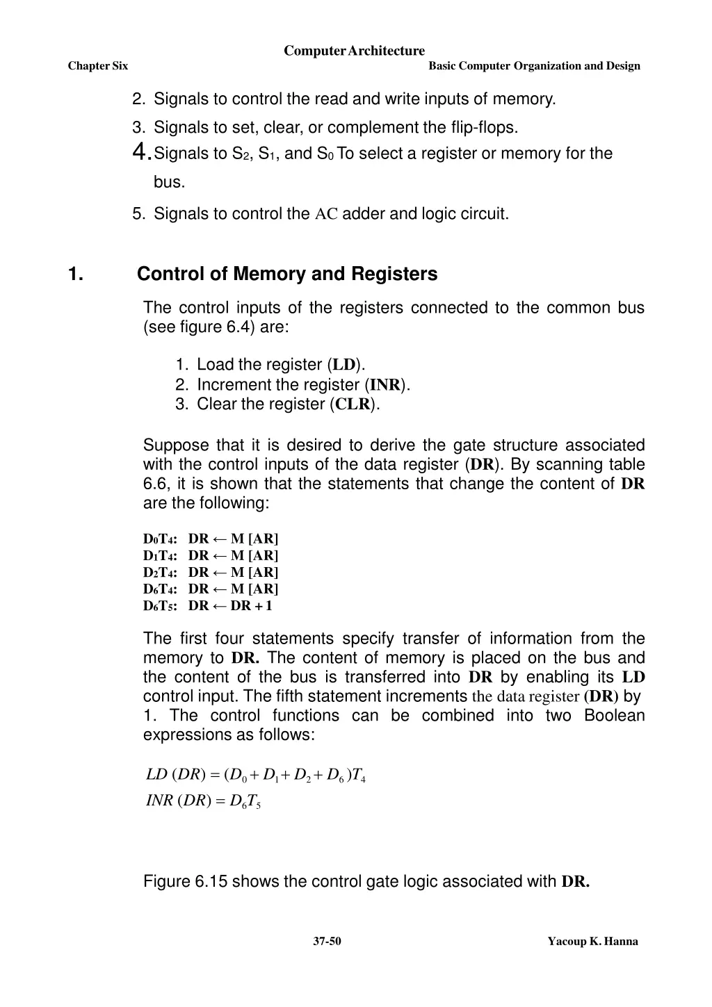
ComputerArchitecture ChapterSix Basic Computer Organization and Design 2. Signals to control the read and write inputs of memory. 3. Signals to set, clear, or complement the flip-flops. 4.Signals to S2, S1, and S0 To select a register or memory for the bus. 5. Signals to control the AC adder and logic circuit. 1. Control of Memory and Registers The control inputs of the registers connected to the common bus (see figure 6.4) are: 1. Load the register (LD). 2. Increment the register (INR). 3. Clear the register (CLR). Suppose that it is desired to derive the gate structure associated with the control inputs of the data register (DR). By scanning table 6.6, it is shown that the statements that change the content of DR are the following: DR M [AR] DR M [AR] DR M [AR] DR M [AR] DR DR +1 D0T4: D1T4: D2T4: D6T4: D6T5: The first four statements specify transfer of information from the memory to DR. The content of memory is placed on the bus and the content of the bus is transferred into DR by enabling its LD control input. The fifth statement increments the data register (DR) by 1. The control functions can be combined into two Boolean expressions as follows: LD (DR) = (D0+ D1+ D2+ D6)T4 INR (DR) = D6T5 Figure 6.15 shows the control gate logic associated with DR. 37-50 Yacoup K.Hanna
ComputerArchitecture ChapterSix Basic Computer Organization and Design Figure 6.15 In similar way, one can derive the control gates for the other registers as well as the logic needed to control the read and write inputs of memory. The logic gates associated with the write input of memory is derived by scanning table 6.6 to find the statements that specify a write operation. Note that the write operation is recognized from the symbol M [AR] . Write = RT1+ D3T4+ D5T4+D6T6 Figure 6.16 shows the control gate logic associated with Write input of the memory. Figure 6.16 38-50 Yacoup K.Hanna
ComputerArchitecture ChapterSix Basic Computer Organization and Design 6.9.1.2. Control of Single Flip-Flops In similar manner, the control gates for the seven flip-flops S, E, R, IEN, FGI, FGO, and I can be determined. Example Show the complete logic control of the IEN Flip-flop in the basic computer. Use a JK flip-flop for this purpose. Solution By scanning table 6.6, it is shown that the statements that change the state of the Flip-flop IEN are the following: pB7: IEN 1 pB6: IEN 0 RT2: IEN 0 Where p = D7 IT3 and B6 and B7 are bits 6 and 7 respectively. Using JK flip-flop for the IEN, the complete control logic will be as shown in figure 6.17. Figure 6.17 39-50 Yacoup K.Hanna
ComputerArchitecture Chapter Six Basic Computer Organization and Design 6.9.1.3. Control of Common Bus As explained before, the 16-bit common bus is controlled by the three selection inputs S2, S1, and S0 (see figure 6.4). To select any one of the registers or the memory, a binary number equivalent to the decimal number shown with each bus input must be applied to the selection inputs S2, S1, and S0 in order to select the corresponding register or memory. Table 6.7 is recognized as the truth table of a binary encoder, which specifies the binary numbers for S2S1S0 that select each register or memory. Each binary number is associated with a Boolean variable X1 to X7, corresponding to the gate structure that must be active in order to select the register or memory for the bus. As an example, when X3 = 1, the corresponding value of S2S1S0 must be 011 and the output of DR will be selected for the bus. Table 6.7 Selected Register for the Bus None AR PC DR AC IR TR Memory Inputs Outputs S2 S1S0 0 0 0 0 0 1 0 1 0 0 1 1 1 0 0 1 0 1 1 1 0 1 1 1 X1 X2 X3 X4 X5 X6 X7 0 0 0 0 0 0 0 1 0 0 0 0 0 0 0 1 0 0 0 0 0 0 0 1 0 0 0 0 0 0 0 1 0 0 0 0 0 0 0 1 0 0 0 0 0 0 0 1 0 0 0 0 0 0 0 1 Figure 6.18 shows the encoder at the inputs of the bus selection logic. The Boolean functions for the encoder are as follows: S0= X1+ X3+ X5+ X7 S1= X2+ X3+ X6+ X7 S2= X4+ X5+ X6+ X7 40-50 Yacoup K.Hanna
ComputerArchitecture ChapterSix Basic Computer Organization and Design Figure 6.18 How to determine the control logic for each encoder input Suppose that it is required to find the control logic that makes X2= 1 and S2S1S0= 010 (select the register PC as the source register). We proceed as follows: 1. Scan all register transfer statements in table 6.6 and extract those statements that have PC as a source register. AR PC RT0 : RT0: TR PC D5T4 : M[AR] PC 2.The Boolean function for X2 is: X 2 = RT0 + RT0 + D5T4 3.Draw the control logic for X2 (Figure6.19). Figure 6.19 In a similar manner, one can determine the gate logic for other registers or memory. Homework Find the control logic that makes X1 = 1 and S2S1S0 = 001 (select the register AR as the source register). 41-50 Yacoup K.Hanna
ComputerArchitecture Chapter Six Basic Computer Organization and Design 2. Design of Accumulator Logic Figure 6.20 presents the circuit block diagram associated with the accumulator register (AC). The adder and logic circuit has three inputs: 1. 16-bit inputs from the outputs of the accumulator register (AC) it self. 2. 16-bit inputs from the data register DR. 3. 8-bit inputs from the input register INPR. The output of the adder and logic circuit provides the data inputs for the accumulator register (AC). In addition, it is necessary to include in the design the logic gates for controlling the LD, INR, and CLR of the register and the controlling operation of the adder and logic circuit. Figure 6.20 42-50 Yacoup K.Hanna
ComputerArchitecture Chapter Six Basic Computer Organization and Design 6.9.2.1. Control of Accumulator Register In the same manner in order to design the logic that controls the accumulator register AC, it is necessary to scan all register transfer statements in table 6.6 and extract those statements that change the content of AC. These register transfer statements are: From the control functions in the list above, the gate configuration is derived as follows: 1. The control function for the increment microoperation (INR) is rB5, where r = D7I T3and B5= IR(5). 2.The control function for the clear microoperation (CLR) is rB11, where r = D7I T3and B11= IR(11). 3. The control function for the load microoperation (LD) is the result of the remaining seven generated in the adder and logic circuit and are loaded at the proper time. microoperations, which Figure 6.21 shows the gate structure that controls the LD, INR, and CLR inputs of the accumulator register AC. Note that the outputs of the gates for each control function are marked with a symbolic name. 43-50 Yacoup K.Hanna
ComputerArchitecture ChapterSix Basic Computer Organization and Design Figure 6.21 2. Adder and Logic Circuit Figure 6.22 shows the internal construction of the accumulator register AC. Each stage has a JK flip-flop, two OR gates, and two AND gates. The load (LD) is connected to the inputs of the AND gates. Figure 6.23 shows one stage of AC register (here the OR gates are removed) since the other functions (i.e. Clear and Increment of the register AC are not included). When LD input is enabled, the 16 inputs Iifor i = 0,1,2, , 14,15 are transferred to AC (0-15). Every stage of Adder and Logic Circuit consists of: 1. Seven AND gates, every one has one of its inputs one of the functions comes from figure 6.21 as an enable. For example, the input named DR in figure 6.23 connected to the output marked DR in figure 6.21. 2. One OR gate. 3. One Full-adder (FA). 44-50 Yacoup K.Hanna
ComputerArchitecture ChapterSix Basic Computer Organization and Design How the arithmetic and logic operations are achieved? 1 . ADD operation This operation achieved using a binary full-adder having their two inputs from the corresponding bits (i) of registers AC and DR, the input carry from the previous stage, and the result transfers through OR gate to register AC, and the output carry to next stage or to the E flip-flop when this stage is the last stage. 2 . AND operation The AND operation is obtained through ANDing AC (i) with the corresponding bit in the data register DR (i), and the result transfers through OR gate to register AC. Figure 6.22 45-50 Yacoup K.Hanna
ComputerArchitecture ChapterSix Basic Computer Organization and Design 3 . Transfer the content of the register DR When DR input is active, the content of the register DR transferred to the registerAC. 4 . Transfer the content of the register INPR When INPR input is active, the 8-bits of the register INPR transferred to Bits 0-7 of the accumulator register AC. 5 . Complementation of the contents of AC register When COM input is active, the content of register AC is inverted and re-transferred to the register. 6 . Shift-right operation This operation transfers bit AC ( i+1 ) into bit AC ( i ). 7 . Shift-left operation This operation transfers bit AC ( i -1 ) into bit AC ( i ). Figure 6.23 46-50 Yacoup K.Hanna
ComputerArchitecture ChapterSix Basic Computer Organization and Design Problems of Chapter Six Q1. A computer uses a memory unit with 256 words of 32 bits each. A binary instruction code is stored in one word of memory. The instruction has four parts as follows: a. Indirect bit. b. Operation code. c. Register code part to specify one of 64 registers. d. Address part. (1) How many bits are there in: (a) The operation code. (b) The register code part. (c) The address part. (2) Draw the instruction word format and indicate the number of bits in each part. (3) how many bits are there in the data and address inputs of the memory. Q2. What is the difference between a direct and indirect address instruction? How many references to memory needed for each type of instructions to bring an operand into a processor register? Q3. The following control inputs are active in the bus system shown in figure 6.4. For each case, specify the register transfer that will be executed during the next clock transition. SelectionInput S1 S2 S3 1 1 1 1 1 0 0 0 LD Memory Adder of Register IR PC DR AC 1 0 0 0 Read - Write - - - - Add Q4. The content of AC in the basic computer is hexadecimal A937 and the initial value of E is 1. Determine the contents of AC, E, PC, AR, and IR in hexadecimal after the execution of the CLA instruction. Repeat 11 more times, starting from each one of the registers-reference instructions. The initial value of PC is hexadecimal 021. 47-50 Yacoup K.Hanna
ComputerArchitecture Chapter Six Basic Computer Organization and Design Q5. An instruction at address 021 in the basic computer has I = 0, an operation code of the AND instruction, and an address part equal to 083. The memory word at address 083 contains the operand B8F2 and the content of AC is A937. Go over the instruction cycle and determine the contents of the following registers at the end of the execute phase: PC, AR, DR, AC, and IR. Repeat the problem six more times starting with an operation code of another memory- reference instruction. Q6. Show the contents in hexadecimal of registers PC, AR, DR, IR, and SC of the basic computer when an ISZ indirect instruction fetched from memory and executed. The initial content of PC is 7FF. The content of memory at address 7FF is EA9F. The content of memory at address A9F is 0C35. The content of memory at address C35 is FFFF. Give the answer in a table with five columns, one for each register and a row for each timing signal. Show the contents of the registers after the positive transition of each clock pulse. Q7. The content of PC in the basic computer is 3AF. The content of AC is 7EC3. The content of memory at address 3AF is 932E. The content of memory at address 32E is 09AC. The content of memory at address 9AC is 8B9F. a. What is the instruction that fetched and executed next? b. Show the binary operation that performed in the AC when, the instruction is executed. c. Give the content of registers PC, AR, DR, AC, and IR in hexadecimal and the value of E, I, and the sequence counter SC in binary at the end of the instruction cycle. Selected problems from chapter 5 in the text forexa. P1. The following control inputs are active in the bus system shown in fig. 5-4. for each case, specify the register transfer that will be executed during the next clock transition. S2 S1 S0 LD of Register Memory adder a. 1 1 1 IR b. 1 1 0 PC c. 1 0 0 DR d. 0 0 0 AC Read - Write - - - - Add P2. The following register transfers are to be executed in the system of fig. 5-4. a. b. c. d. AR PC IR M[AR] M[AR] TR AC DR, DR AC Done simultaneously 48-50 Yacoup K.Hanna


