Understanding Latch-Up and Guard Rings in Digital Chip Design
Explore the typical structure of a digital chip, latch-up layout rules, over-voltage risks in I/O circuits, and the injection of minority carriers affecting chip functionality. Learn about the importance of guard rings in protecting against latch-up phenomena.

Download Presentation

Please find below an Image/Link to download the presentation.
The content on the website is provided AS IS for your information and personal use only. It may not be sold, licensed, or shared on other websites without obtaining consent from the author. If you encounter any issues during the download, it is possible that the publisher has removed the file from their server.
You are allowed to download the files provided on this website for personal or commercial use, subject to the condition that they are used lawfully. All files are the property of their respective owners.
The content on the website is provided AS IS for your information and personal use only. It may not be sold, licensed, or shared on other websites without obtaining consent from the author.
E N D
Presentation Transcript
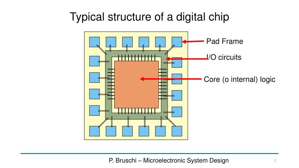
Typical structure of a digital chip Pad Frame I/O circuits Core (o internal) logic P. Bruschi Microelectronic System Design 1
Latch-up layout rules: core logic Every part of a p-active area in an n-well must "see" at least one well- tap with a maximum distance R Every part of an n-active area in the substrate (p- well) must "see" at least one substrate-tap with a maximum distance R P. Bruschi Microelectronic System Design 2
I/O circuits: over-voltage risk Real case possible load / transmission line equivalent circuit Ideal case Vout Vdd I/O pad gnd In I/O circuits, the output termination can exceed the Vdd or gnd rails. This introduces additional risk of latch-up P. Bruschi Microelectronic System Design 3
Injection of minority carriers when Vout exceeds Vdd, this diode is turned on when Vout drops below gnd, this diode is turned on Well: bases of the pnp BJT (collector of npn BJT) Substrate: bases of the npn BJT (collector of pnp BJT) P. Bruschi Microelectronic System Design 4
Injection of minority carriers Injection of minority charge carriers into the parasitic BJTs bases may trigger the latch-up phenomenon Electron injection into the substrate when Vout< 0 Hole injection into the n-well when Vout > Vdd P. Bruschi Microelectronic System Design 5
I/O devices: Guard Rings I/O circuits require additional protection against latch-up Guard rings are placed around the I/O devices in order to: Reduce the resistance between drain/body diffusions to gnd (nMOS) or Vdd (pMOS) Collect most of the minority carriers injected by one device before they reach neighboring devices n-well p+ (sub-tap) I/O devices n+ (well tap) p+ (sub. tap) gnd vdd vdd gnd These guard rings further reduce the effects of the I/O devices on the core logic n-well vdd p+ (sub. tap) gnd P. Bruschi Microelectronic System Design 6