Understanding Noise in Active Devices: MOSFETs Schematics & Analysis
Explore the principles of noise in active devices, focusing on MOSFETs, with valid schematics and frequency-dependent models. Learn about thermal noise, flicker noise, and the relationship between noise expressions in MOSFETs. Discover equivalent gate noise and the equivalence between output-referred and input-referred noise models in microelectronic system design.

Uploaded on | 1 Views
Download Presentation

Please find below an Image/Link to download the presentation.
The content on the website is provided AS IS for your information and personal use only. It may not be sold, licensed, or shared on other websites without obtaining consent from the author. If you encounter any issues during the download, it is possible that the publisher has removed the file from their server.
You are allowed to download the files provided on this website for personal or commercial use, subject to the condition that they are used lawfully. All files are the property of their respective owners.
The content on the website is provided AS IS for your information and personal use only. It may not be sold, licensed, or shared on other websites without obtaining consent from the author.
E N D
Presentation Transcript
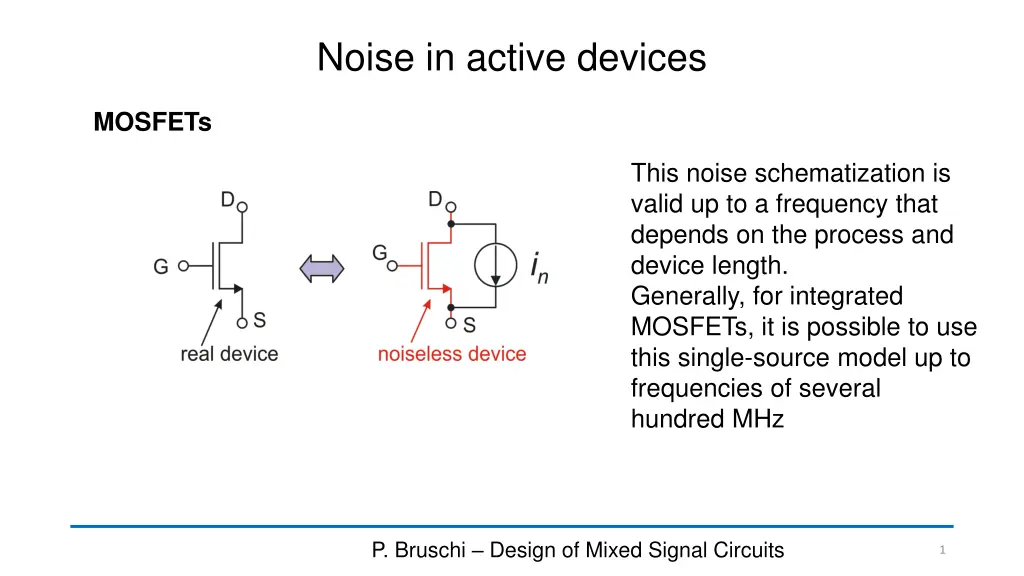
Noise in active devices MOSFETs This noise schematization is valid up to a frequency that depends on the process and device length. Generally, for integrated MOSFETs, it is possible to use this single-source model up to frequencies of several hundred MHz P. Bruschi Design of Mixed Signal Circuits 1
Mosfet Thermal noise 8 3 = ( ) f S kTg m Typically: In T m g 1 1.5 m = + 1 mB g m m Being frequency independent, thermal noise is the origin of the broad-band noise in MOSFETs A more general expression: = ( ) 4 S f kTg In T n m 1 R 2 3 = = 4 4 S kT kTG = 1 m In R n P. Bruschi Microelectronic System Design 2
Mosfet flicker noise Frequently used by designers of analog integrated circuits N 1 f f = 2 m ( ) S f g In F WL Nfis a parameter that depends on the process N-MOS: Nfn P-MOS: Nfp ( m) 2 2 V Dimensions of Nfare: k I C 1 f A more general expression of the flicker PSD (can be used in SPICE) fi = ( ) f S In F 2 eff L OX P. Bruschi Microelectronic System Design 3
Relationship between the two noise expressions N 1 f = 2 g I f = 2 m ( ) S f g m D In F WL 2 N WL f N C I 1 1 f W L f f OX = ( ) f 2 = S C I In F OX D 2 L k = = k I C 1 1 1 f fi =2 N fi = ( ) f S f 2 OX In F C 2 eff L OX P. Bruschi Microelectronic System Design 4
Equivalent gate noise ? Substituting inwith a single voltage source in series with the gate gives a contribution that depends on the resistance (R) seen by the gate. 1 = = = dn i i dn i m gs g v m n g v n + 1 j Rc gs P. Bruschi Microelectronic System Design 5
Equivalence between the output referred and input referred noise models input referred model output referred model v + gn i R j Rc 1 1 n = g = dn i g v i m 1 m n gn + + j c 1 1/ j Rc R gs gs gs Independent of R, as required for the equivalence with the output referred model, which results in: dn i By setting: = j c v = i dn i v g = i gn gs n n m n P. Bruschi Microelectronic System Design 6
Equivalence between the output referred and input referred noise models = j c v i gn gs n i = n v = i v g n g n n m m Note that ignis dependent on vn (they are correlated stochastic processes) P. Bruschi Microelectronic System Design 7
Transformations between drain noise current and gate noise voltage i = = i v g n v n n m n g m ( ) 2 m g S f ( ) f ( ) f ( ) f = = In 2 m S S g S In Vn Vn 8 3 N WL f 1 8 3 = ( ) f Vn T S kTmg 1 f = ( ) f S kTg m Thermal noise: In T m m N 1 f = ( ) f Vn F S f = 2 m ( ) S f g Flicker noise: In F WL P. Bruschi Microelectronic System Design 8
Noise in BJTs Since the BJT has a non negligible base current, it is necessary to use two distinct current noise sources for the base and the collector Simplified BJT noise model Collector noise current Base flicker noise = 2 S qI I InC C = 2 + B S qI k InB B fB f Only shot noise (broad-band) Base shot noise (broad-band) P. Bruschi Microelectronic System Design 9
MOSFET vs BJT Let us consider only the drain (in) and collector (inc) noise sources. = 2 3 n MOS ( ) f 4 S kTg = 2 S qI In T m InC C kT q I V n MOS = 1 m = = = I m T g V g C g C m m T 2 kT q 1 2 = = 2 S qg kTg n BJT = = n BJT ( ) f 4 S kTg InC m m InC m P. Bruschi Microelectronic System Design 10
BJT input referred noise voltage nC i g = v n 1 z 1 r + j c m v z be = n bn v i in be in + v v v if z R be S n in S The noise voltage source vnis the only significant contribution to the input referred noise V I 1 = = 2 kT T 2 S kTg BJT: Vn C m 1 g V Much more noise for the same static current consumption! = 4 4 S kT kT TE I MOSFET Vn m D P. Bruschi Microelectronic System Design 11
The Noise Efficiency Factor (NEF) Since the single-BJT amplifier offers an excellent trade-off between noise and power consumption, in 1987 M. Steyaert (KU Leuven University) proposed a FOM (figure of merit) called NEF to characterize all voltage amplifiers in terms of noise efficiency Total rms noise of the amplifier under consideration rms rti V = NEF V 4 kT B T Effective noise bandwidth and total current consumption of the amplifier under consideration 2 I supply Denominator = 2 rms bjt V Input rms voltage of a BJT with same current and BW of the amplifier P. Bruschi Microelectronic System Design 12


")