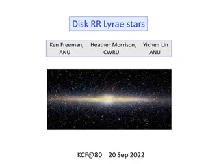
Unveiling Galactic Center: Infrared Quintuplet Discovery
The Galactic center harbors obscured objects revealed through infrared and radio observations. Learn about the discovery of the Infrared Quintuplet, unveiling hidden stars and gas near the supermassive black hole.

Download Presentation

Please find below an Image/Link to download the presentation.
The content on the website is provided AS IS for your information and personal use only. It may not be sold, licensed, or shared on other websites without obtaining consent from the author. If you encounter any issues during the download, it is possible that the publisher has removed the file from their server.
You are allowed to download the files provided on this website for personal or commercial use, subject to the condition that they are used lawfully. All files are the property of their respective owners.
The content on the website is provided AS IS for your information and personal use only. It may not be sold, licensed, or shared on other websites without obtaining consent from the author.
E N D
Presentation Transcript
Most objects in the center of the Milky Way are so highly obscured from our view by intervening dust that, at wavelengths visible to the naked eye, only about one photon out of every trillion emitted by them toward the Earth actually reaches our planet. This makes it impossible to observe the copious visible light emitted by the Galactic center s stars, hot gas, the accretion disk encircling the supermassive black hole, and many other objects. The amount of obscuration decreases rapidly with increasing wavelength and thus most of our information about the Galactic center s resident objects and gas comes from infrared and radio observations. For some Galactic center stars, those that are embedded in dust shells of their own making, the obscuration is even more extreme. Among these are five infrared-luminous objects known as the Infrared Quintuplet, located at the center of a cluster of hundreds of hot and massive stars, which has been given the name Quintuplet Cluster. The Quintuplet Cluster is only 30 parsecs (100 light years) distant from the central massive black hole at the very center of our galaxy. J-band spectra of three of the five members of the Infrared Quintuplet showing emission lines of neutral helium and ionized carbon. The continuum radiation from the stars and their dust shells actually decrease rapidly from longer to shorter wavelengths and is barely detectable at the short wavelength edge of these spectra. In the figure the spectra have been flattened to more easily reveal the line emission. The increasing noisiness of the spectra toward their short wavelength edges demonstrates the increasing difficulty of detecting any light at all from these objects at those wavelengths. The difficulty in observing these five stars is greater, not only due to the additional obscuration by their dust shells, but also because the shells are warmed by their central stars and emit bright infrared continuum radiation, diluting any infrared light from the stars themselves. The combination of these effects has made it very challenging, if not impossible, at any infrared wavelength to detect light from the interiors of the shells leaking through the dust cocoons and surviving the journey through the interstellar dust to our telescopes, or so it was thought. Thus, little has been learned about natures of these objects since they were discovered over a quarter century ago. The only clues were high-resolution infrared images which showed that the dust emission from two of the five resembled pinwheels. Previously this phenomenon had only been seen outside of the Galactic center, in a few objects identified as Wolf-Rayet colliding wind binaries, which are double star systems comprised of extremely luminous hot stars with massive winds. Several years ago, while using NIFS at Gemini North for an unrelated research program, Tom Geballe serendipitously discovered a very faint and broad emission line due to hot helium gas near 1.7 microns in the infrared spectrum of one of the Quintuplet stars. Prompted by this, a team consisting of him, Paco Najarro (Centro de Astrobiolog a, Spain), Don Figer (Rochester Institute of Technology), and Diego de la Fuente (Universidad Nacional Aut noma de M xico) successfully proposed to use NIFS and GNIRS to obtain sensitive spectra of all five members of the infrared Quintuplet, not only near 1.7 microns, but also down to wavelengths as short as 1.0 micron. Near the short end of that wavelength range, one photon in several thousand survives the journey first through the dust cocoon and then from the Galactic center to Earth. That fraction is much larger than the one in a trillion at visible wavelengths, but is still tiny. However, the contaminating emission from the warm dust shells is greatly reduced, increasing the contrast between any spectral features emitted from inside the dust shells and the continuum emission from the shells themselves. Thus, the team reasoned that with a large telescope, a sensitive spectrograph, and less dilution from the warm dust, they would be able to detect the faint light coming from within the cocoons. The spectra, recently published in The Astrophysical Journal, reveal the presence of emission lines from four of the five members of the Quintuplet, and have allowed us to definitively identify the four as containing late-type, carbon-rich Wolf-Rayet stars, as was suspected based on the earlier imaging. These massive stars are only a few million years old, but have completely lost their outer hydrogen-rich layers and probably do not have much longer to exist before exploding violently as supernovae.
RIT, FIT Camera Being Tested on ISS ROCHESTER, N.Y. Imaging technology advanced by researchers at the Rochester Institute of Technology (RIT) and the Florida Institute of Technology (FIT) is being tested on the International Space Station (ISS) and could someday be used on future space telescopes. A new twist on the charge injection device (CID) camera, originally developed in 1972 by General Electric Co., fine-tunes the array of pixels for improved exposure control in low-light conditions. The enhanced technology could give scientists a new method for imaging planets around other stars and improve the search for habitable Earth-like planets. Zoran Ninkov, professor at RIT's Chester F. Carlson Center for Imaging Science, and Daniel Batcheldor, head of physics and Space Sciences at FIT, designed the charge injection device camera to capture contrasts between light emitted by astronomical objects. "CID arrays offer considerable promise in many applications due to the focal plane architecture that allows random pixel access and nondestructive readout," Ninkov said. In addition to improving presently available devices, the development of next-generation imaging arrays promise considerable flexibility in read-out and on-chip processing for the future." A SpaceX Falcon 9 rocket carried the charge injection device to the ISS in the cargo of supplies and science experiments in February. Astronauts have installed the camera on a platform outside the space station and will test the camera for six months. "We expect to start seeing results by the end of April," Batcheldor said. "A complex test pattern will be sent from a successfully operated camera through the ISS systems and down to the ground. A successful demonstration of CIDs on the International Space Station will put this technology at the NASA Technology Readiness Level 8, which means it's ready to fly as a primary instrument on a future space telescope."
Data Centers and Telecommunications Data Centers and Telecommunications Integration and packaging of optical components such as laser sources, multiplexers, detectors and modulators into a single chip are ushering in a new era of communications to 100 Gbps and beyond. Today s data centers deliver millions of services, processing terabytes of data per second around the world for billions of devices. Considering the volume, it s amazing that we ever have a signal. As the need for connectivity increases, data centers are under constant pressure to add more and more massive racks of servers and fiber optic interconnects, which takes money and time, energy and real estate. This false color 3D atomic force microscope image shows the height profile of the InAs QDs on Si The demand for large-scale cloud computing and ever-faster processing is growing so fast that network traffic in data centers is doubling every twelve months, according to Diane Bryant, vice president and general manager of data centers at Intel.1 And copper wires struggle to transmit at data rates of 25 Gbps over a few meters, says Microsoft s general manager of hardware engineering, Kushagra Vaid. As data rates start getting to 100 Gbps and this will happen in the future we are going to hit a brick wall, Vaid said. Figure 5b. Figure 5b. This false color 3D atomic force microscope image shows the height profile of the InAs QDs on Si (at left). Figure 5c. Figure 5c. The Si PIC generates optical time- division multiplexing signals at 40 Gbps from 10 Gbps QD mode-locked lasers (right). The circuit splits the short pulses from the laser into four separate paths, each modulated by Si ring resonator electro-optic modulators, delayed and recombined at the higher data rate of 40 Gbps. Courtesy of K. Tian and Z. Wang, RIT and M. Fanto, RIT. PICture PICture this this One of the steepest challenges to widespread adoption of PICs (photonic integrated circuit) is incorporating lasers into the chip. More than one material may emerge as a winner for use in hybrid lasers on PICs. Silicon itself doesn t lase, although adding a layer of a III-V material helps overcome that limitation; Intel added InP, for example. But III-V materials are inherently not compatible with conventional CMOS fabrication, leading to expensive work-arounds. Research is hot on the trail of graphene, a two-dimensional layered material that can emit, transmit and detect photons, but issues of CMOS scalability and performance are handicaps that will take time to overcome4. One lasing material showing great promise is quantum dots (QDs) (Figure 5). Recently, researchers at Rochester Institute of Technology (RIT, Rochester, N.Y.) demonstrated that indium arsenide (InAs) QD laser heterostructures can successfully be grown and transferred to Si substrates via a low-temperature palladium (Pd)-mediated wafer bonding process (Figure 5a, 5b). Associate professor of microsystems engineering Stefan Preble and colleagues at RIT, in collaboration with professor Wei Guo at the University of Massachusetts, Lowell, further demonstrated mode-locking of these lasers, which would enable stable optical pulse trains of short pulses (<10 ps) at high repetition rates for optical time-division multiplexing (OTDM), among other uses (Figure 5c)5. The group is looking at schemes to combine wavelength division multiplexing (WDM) with OTDM to get to data rates beyond 400 Gbps. The biggest hurdle with QDs is efficiency, but their temperature stability is making them hot prospects for next-generation PICs. Quantum dots have recently been pulling ahead of quantum wells as a promising next-gen PIC solution, said Preble. The QD is less susceptible to defects that destroy performance over time. And several promising approaches for direct growth of QDs on Si chips are emerging. But the yield and long-term reliability of QDs on silicon remains to be proven. Other schemes beyond WDM and OTDM may someday be able to carry terabyte data rates on a single chip. Assistant professor of electrical engineering Liang Feng at the University at Buffalo, State University of New York, and colleagues recently demonstrated a tiny microring laser that emits photons in a radially polarized stream. The orbital angular momentum (OAM) of the photons creates a vortex shape that offers novel degrees of freedom and flexible control through on-demand topological charge and polarization states. The scheme may enable mode multiplexing over many orders (potentially an infinite number of orders) for tens of OAM channels6,7,8 (Figure 6). The OAM laser might offer entirely new ways of implementing high-speed, secure optical signals in both classical and quantum regimes. Fifty years ago you couldn t have imagined what our everyday life would be like today, said Feng. The power in our laptops is as great as the supercomputers that helped put astronauts on the moon. We certainly have a very long way to go, but all over the world people are trying to increase the laser energy emission in photonic circuits. In the next 50 years, it s exciting to imagine what we ll accomplish.
How does any ship, from watercraft to spacecraft, successfully navigate away from the sight of natural landmarks on the Earth s surface? By using the stars. By using the stars. A team of engineering undergraduates at the Rochester Institute of Technology (RIT) are reaching for those stars with a new research project for NASA: designing a compass for rockets using a new type of detector technology. What these engineers are working to design, build and eventually deploy is a star-tracking system for rocket navigation. Intended to fly on a NASA technology demonstration mission later in the year, the system combines telescope and camera components that will orient rocket payloads based on images of the visible star field. Star Star- -Tracking Navigation Systems with New Cryogenic Materials Tracking Navigation Systems with New Cryogenic Materials Star-tracking systems have been used for satellite, rocket and other spacecraft navigation for quite some time. What sets this project apart is revealed in its name: the Cryogenic Star Tracking Attitude Regulation System (CSTARS). The RIT students are experimenting with detectors made of metal-oxide semiconductors (CMOS), which show promise to operate well even at temperatures as cold as that of liquid nitrogen, minus 320 degrees Fahrenheit. Being able to operate at super-low temperatures is important for space systems, as the cryogenic temperatures reduce dark current in the sensors and increase instrument sensitivity. The traditional technology used in astronomical imagine systems is often similar to that found in consumer electronics charge-coupled detectors (CCDs) which become inoperable at very cold temperatures. The prototype from RIT is a move toward developing fully cryogenic detectors that could improve the sensitivity of NASA s future deep-space cameras. The star tracker will fly as part of a technology demonstration payload on a suborbital sounding rocket launching from NASA s Wallops Flight Facility in December of this year. The aim is to control this sensor and make it work at cold temperatures, said Kevin Kruse, a fifth-year electrical engineering student and the team leader. Then we ll launch it into space to take pictures. A future mission would involve us guiding the rocket using the images we take. Engineering Undergrads Build Their Skills with NASA Projects The project at RIT is funded with a $200,000 grant from NASA s Undergraduate Student Instrument Project (USIP) Flight Research Opportunity program, which provides research grants specifically to undergraduate- led teams. The program is geared to supporting the development of professional engineering skills in undergraduate engineering students. It also gives these students the valuable experience that comes from creating experiments directly relevant to NASA missions. The students on the team hail from a range of engineering disciplines. Members include electrical, mechanical and computer engineering undergraduates. They are also working with team members from other departments at RIT, including physics, computational mathematics and business. This type of interdisciplinary team environment enhances the experience and skills these students learn by creating an experience the same as how teams in future professional projects will operate. Between the high-level technical skills students develop through these kinds of programs, as well as the leadership and teamwork skills that come from collaborative projects, these engineers will have great experiences to bring with them into graduate school or their future career.
Solar Power for Everyone Solar Power for Everyone Researchers at the Rochester Institute of Technology (RIT) are taking an unconventional approach to improving efficiency and lowering the cost of solar cell technology in the ongoing quest for feasible ways to reduce the reliance on a complex electrical infrastructure. Parsian Mohseni, assistant professor in RIT's Kate Gleason College of Engineering, is co-principal investigator, leading a team conducting research using nanowire to capture more of the sun s energy instead of traditional film. He said that if trends go as expected, anyone with solar cells may be able to use them in their home while sending excess energy back to the grid. Consumers can also use the devices on-the-go, by taking them out of a backpack or attaching them to the roof of a car. The idea is they can produce their own power wherever they are, whether at home or on the go, Mohseni said. Today s solar panels convert the sun's rays into electricity by exciting electrons in silicon cells using the photons of light from the sun. Silicon has remained the current conductive material of choice in most electronic devices because of its low cost, simple processing, and useful temperature range. But with the demand for more storage, better conductivity, lower prices, and higher power for new technologies such as photonics and higher speed transistors, researchers are looking to supplement silicon with other materials that can meet those needs. Mohseni s team is building on work previously done that uses a combination of different types of materials, from Group Three and Five on the periodic table, and a different process for better conductive capabilities. But those materials are so expensive that they are used only in special applications, such as space technologies, and not for solar panels and other consumer products. Researchers began considering using these materials, a combination of metallic and non-metallic elements, around 1990. It was a really novel approach then, Mohseni says. After some work, they realized they could get superior performance compared to any other existing solar cell technologies, but it remained too costly for everyday use. Mohseni s team began exploring ways to cut costs. One way is through the use of nanowires. The ultra-thin, grass-like vertical structures, they found, could be used as a replacement for the thin films made from silicon. The nanowires reduce the amount of material used in the devices and decreases costs by nearly 90 percent. When using film, Mohseni explained, the material has to be thick to capture more light, because when the light isn t absorbed, it will bounce or reflect off of the film. Nanowires act differently. If light bounces off one wire in an array, it can be captured by a nearby wire and re-absorbed. This effect of multiple scattering interactions increases the light-trapping capabilities of the nanowire array. Even though we are using 90 percent less material, we can absorb light better than a thin-film structure," he added. It s a luxury that using nanowires provides for us. Mohseni was recently awarded about $300,000 for an Early Concepts Grant for Exploratory Research (EAGER) from the National Science Foundation. The award is designed to support exploratory early-stage work on untested but potentially transformative research ideas or approaches The grant gives the team two years to advance the field. During the two-year window, our goals are to realize high- quality nanowire growth on silicon. Our goals then continue on to characterize these materials to take advantage of them for solar cell applications, he says. We want to characterize their structure, their optical properties, and their electrical properties, and learn how their composition or their spacing or their size modifies these properties. That s the materials exploration side of it. On the engineering side, the team will study how to take advantage of these properties we ve uncovered and make better solar cells. Then the last part is to fabricate solar cells that allow us to realize high efficiencies, all at a significantly lower cost than conventional technologies require, he noted. Mohseni hesitates to talk about a specific timetable because of so many factors beyond his control. It s not a simple question to answer, he says. But he hopes it will be within the next decade that, We are going to be independent of fossil fuels.
RIT engineering faculty Jing Zhang awarded NSF grant for high RIT engineering faculty Jing Zhang awarded NSF grant for high- -tech nanofabrication equipment Plasma reactive ion etching system to be integrated into RIT s clean room and used for photonics and Plasma reactive ion etching system to be integrated into RIT s clean room and used for photonics and nanoelectronic nanoelectronic device research and development device research and development tech nanofabrication equipment Jing Zhang, engineering faculty member at Rochester Institute of Technology, received a $305,000 grant from the National Science Foundation to acquire a new etching system for photonic, electronic and bio-device fabrication. The system strengthens RIT s fabrication capability in its Semiconductor & Microsystems Fabrication Laboratory to support new and existing multidisciplinary research in science and engineering, to enable educational curriculum development, and be used for workforce development and training activities led by RIT s engineering college. The ICP-RIE system an inductively coupled plasma reactive ion etching system is equipment used to create specific structural patterns, or to expose different conductive layers, on the integrated circuits found in electronic devices, said Zhang. Jing Zhang, engineering faculty member at Rochester Institute of Technology, received a $305,000 grant from the National Science Foundation to acquire a new etching system for photonic, electronic and bio-device fabrication. The system strengthens RIT s fabrication capability in its Semiconductor & Microsystems Fabrication Laboratory to support new and existing multidisciplinary research in science and engineering, to enable educational curriculum development, and be used for workforce development and training activities led by RIT s engineering college. The ICP-RIE system an inductively coupled plasma reactive ion etching system is equipment used to create specific structural patterns, or to expose different conductive layers, on the integrated circuits found in electronic devices, said Zhang. If we want to fabricate a wafer into a device, we needed to have this type of etcher, said Zhang, the Kate Gleason Endowed Assistant Professor in the electrical and microelectronic engineering department in RIT s Kate Gleason College of Engineering. There is no equipment like this close by so there was a huge need, and it will help with collaborations we have with other university and corporate researchers. Traditional semiconductor research has focused on silicon-based materials. Zhang is working on compound semiconductors, and gallium nitride is an emerging material being applied. Gallium nitride-based semiconductors are being integrated into optoelectronics, such as LEDs, to power electronics for smart grid applications and power management for electric vehicles, solar applications to harvest solar energy and transfer it into electrical energy. New research in ultraviolet wavelength sensors is an emerging area, she explained. The instrument is essential to enable research and education on III-Nitride-based light emitting diodes and lasers, and other semiconductor devices. We are studying every aspect of this material, from understanding the physics to the realization of novel devices. This equipment will help with that process, said Zhang, who has been at RIT since 2014 and is part of a growing and accomplished group of semiconductor materials and photonics device researchers at the university. She has expertise in the area of ultraviolet and visible light emitting diodes, also referred to as LEDs, and in developing semiconductors for optoelectronic and electronic devices. Plasma reactive-ion etching systems incorporate several steps to the integrated circuit fabrication process. Reactive plasm, deposited onto the wafer, removes and refines excess material to etch or form patterns into the layers of the integrated circuit. These etched micro-nanostructures are the foundation for complex semiconductor devices. The ICP-RIE system provides dry etching capability for various material systems such as compound semiconductors, dielectric materials and metals with fast etching rate, well-controlled selectivity and uniformity. With the emphasis on workforce development in the area of photonics, having the new equipment also provides a key educational opportunity for training. RIT s microelectronic engineering department provides short courses in semiconductor fabrication for area high school and community college teachers and for regional company employees looking to advance knowledge in this area. In the past year, RIT also acquired a metal organic vapor-phase epitaxy system, also referred to as an MOVPE, which grows III-V single crystal materials. The state-of-the-art tool gives researchers the ability to build high-performance optical and electronic devices and will be a key learning and training resource. This capability was once an outsourced to research laboratory partners such as NASA. Today, the in-house functionality provided by this equipment, combined with the ICP-RIE system, is available to RIT researchers as well as the regional Rochester photonics community, including partners in AIM Photonics, Zhang added.