A MOSFET Opamp with an N-MOS Differential Pair

This document presents a detailed design of a MOSFET operational amplifier utilizing an N-MOS differential pair. It includes schematics from DxDesigner, a discussion on bias current setup, and current source management within the circuit. Key parameters are derived from SPICE simulations, highlighting vital elements such as the cascode configuration and output stage design. The focus is on effective biasing techniques and their implications on performance, ensuring a comprehensive understanding of amplifier functionality.

Download Presentation

Please find below an Image/Link to download the presentation.
The content on the website is provided AS IS for your information and personal use only. It may not be sold, licensed, or shared on other websites without obtaining consent from the author.If you encounter any issues during the download, it is possible that the publisher has removed the file from their server.
You are allowed to download the files provided on this website for personal or commercial use, subject to the condition that they are used lawfully. All files are the property of their respective owners.
The content on the website is provided AS IS for your information and personal use only. It may not be sold, licensed, or shared on other websites without obtaining consent from the author.
E N D
Presentation Transcript
A MOSFET Opamp with an N-MOS Dfferential Pair Very-like but not quite your assignment
The Schematic: (DxDesigner Drawing) Startup Set bias current Set cascode Differential pair and current Output stage and load bias voltage mirror
Device Parameter Estimates from SPICE Parameter Table for MOSFET Opamp Example element m1 m10 m12 m13 m14 m15 m18 m2 m20 m3 m9 model nssb nssb nssb nssb nssb nssb nssb nssb nssb nssb nssb vds vgs vth vov id gm ro 0.748 3.368 0.711 0.838 3.078 1.092 0.023 3.156 3.929 3.089 1.654 0.851 0.851 0.711 0.851 1.079 1.092 1.930 0.752 0.023 0.752 0.851 0.547 0.547 0.546 0.547 0.840 0.836 0.559 0.547 0.594 0.547 0.547 0.304 0.304 0.165 0.304 0.239 0.256 1.371 0.205 -0.571 0.205 0.304 3.77E-05 4.12E-05 3.51E-05 3.79E-05 3.51E-05 3.79E-05 5.36E-06 1.89E-05 7.88E-12 1.89E-05 5.63E-05 2.90E-04 3.11E-04 5.01E-04 2.91E-04 3.27E-04 3.31E-04 3.42E-06 2.22E-04 4.17E-13 2.22E-04 4.29E-04 5.54E+05 8.09E+05 5.05E+05 5.92E+05 8.12E+05 6.32E+05 4.34E+03 1.36E+06 1.00E+12 1.36E+06 5.19E+05 m11 m11a m16 m17 m19 m4 m5 m6 m7 m8 pssb pssb pssb pssb pssb pssb pssb pssb pssb pssb 0.478 1.154 1.072 3.070 4.977 0.512 0.579 0.584 0.585 3.346 1.632 1.154 1.072 1.072 3.070 1.048 1.047 1.096 1.096 1.164 0.746 0.793 0.737 0.727 0.781 0.812 0.812 0.741 0.741 0.726 0.886 0.362 0.335 0.344 2.289 0.236 0.235 0.355 0.355 0.437 -4.1E-05 -4.1E-05 -3.5E-05 -3.8E-05 -5.4E-06 -1.9E-05 -1.9E-05 -1.9E-05 -1.9E-05 -5.6E-05 6.34E-05 2.08E-04 1.92E-04 1.99E-04 4.35E-06 1.42E-04 1.42E-04 9.73E-05 9.73E-05 2.35E-04 2.13E+04 6.64E+05 7.27E+05 7.14E+05 9.43E+07 8.52E+05 9.19E+05 1.09E+06 1.10E+06 5.96E+05
Setting the Bias Current You don t have to do this. I give you a current source for your assignment. This is one way to separate the amplifier bias from the exact VDD M16 and M17 are a conventional current mirror with the input side on the left. M12 and M13 are a modified mirror with input on right and output on the left. M12 is 4X wider than M13, probably made by parallel connection of 4 copies of M13. Notice that the body of M12 is connected to the source, not to ground (VSS). ID13 times R is the difference in the overvoltages of M12 and M13. Equating ID13 to ID12 and using KVL, we have: 2 13 4 ( ) OV D K V I R = 2 KV 13 OV This has two solutions: both current and VOV13 are zero or 2 OV D V I R = 13 This means that 1 2 1 R I = D I = = g D 13 2 4 KR 13 m V 13 OV
Starting Up the Bias & Providing Cascode Bias The inverter has a very low gate threshold voltage so its output is only high when the bias voltage is too low. M20 forces current into the top mirror until the output bias voltage is enough to settle to a final value. M10 matches M13 so it is a current source with the same standard value as M13. The current ID10 sets VGS for M11 & M11A (effectively a single transistor) that is used to bias the cascode current mirror.
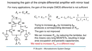
Output Stage at Low Frequency Common Source Amplifier Output load impedance from Channel Length Modulation (r0) in M8 and M9 together with the load and parasitic capacitances Load resistance = Gain proportional to the transconductance of M8 Pole at output: f = ?? || 08 r 07 r ( ) = || G g 08 r 07 r 0 8 m
First Stage: NMOS Differential Pair with Cascoded Current Mirror Output current gain is the transconductance of one of the differential pair transistors (2.22e-4 sie). The current mirror output impedance is the same problem as the Widlar source and the exam problem. ( ) 6 6 7 1 O m O r g r r + + = 1.1 10 ohm 8 7 O The differential pair output resistance is just r0 for one of the differential pair transistors (1.36e6 ohms.) Node impedance is essentially r0 of M3. Gain is 1 3 3 300 X (36 dB) st m O G g r = =
Transfer Function with RM = 0 Zero Bad for phase!!! ( ) 1 / m O g r + sC C r g + = M m ( ) H s ( ) ( ) + + + 2 1 1 s C r C r s m O g r C r C r O o M in M in O O M O Second pole Miller effect Dominant pole
Transfer Function with RM in Place Zero term bad for phase Zero New term good for phase Make RM > 1/gm ( 1 ) + + 1 / m O g r s + sC g sC R C r + = M m M M ( ) H s ( ) ( ) ( ) + + + + 2 1 s C r C r R m O g r C r C r C R O o M in M M in O O M O M M
Where Are the Poles? Denominator polynomial is a quadratic polynomial for which the zeros are: 2 0 as bs c + + = 2 4 b b ac = s p 2 a Using a Taylor series approximation: + + 1 1 if x x x 1 2 1 3 2 2 ac b ac b = 2 4 1 b ac b b 2 b a c b and s s 1 2 p p Pole frequencies show splitting first pole is lowered and second pole is raised from positions without feedback: + 1 2 1 g r m O g r r C = and f f ( ) 2 1 p p + 2 1 r C O O i m O M
What Is the Slew Rate? This circuit has a classic differential input pair (M2 and M3) for high CMRR and low DC drift. It also has a current mirror (M4 M7) with bias from the drain current of M1: IM1Q = 38 amps. A large step input puts all 38 amps into the Miller capacitor CM = 5.5 pf for S.R. = 6.9 V/ sec. VDD IM1Q CM dV I = IM1Q . . S R OUT dt INMAX C IM1Q MAX M -A0 iin = IM1Q vOUT
Final Performance Specifications MOSFET Operational Amplifier Gain and Phase Amplifier Property A0 DC Gain fp dominant pole position fGBW fU unity gain frequency Output stage resistance at low frequency Zero position Slew Rate Output stage quiescent current Opamp quiescent current Bias circuit quiescent current Total system quiescent current VDD Total system power Value 86 DB (X20,000) 400 Hz 8.0 MHz 5.6 MHz 1 00 1 80 80 1 20 Gain Phase 60 60 Phase (deg.) Gain (DB) 277 K 10.7 MHz V/sec 65 a 40 0 7 10 6 20 -60 0 -1 20 103 a 104 a 210 a 5.0 volts 1.1 mW -20 1 .00E+02 -1 80 1 .00E+03 1 .00E+04 1 .00E+05 1 .00E+06 1 .00E+07 1 .00E+08 Frequency (Hz) Phase margin = 60 deg.

")