Bipolar Junction Transistors
Bipolar junction transistors (BJTs) are crucial components in electronic circuits, particularly in amplifier and switching applications. This content delves into the operation and configuration of NPN and PNP BJTs in common base mode, detailing the flow of electrons and holes to generate electric current. The images illustrate how free electrons move from the emitter to the base and then on to the collector, under the influence of bias voltages. By grasping this common base configuration, you can comprehend the functioning of BJTs better.

Download Presentation

Please find below an Image/Link to download the presentation.
The content on the website is provided AS IS for your information and personal use only. It may not be sold, licensed, or shared on other websites without obtaining consent from the author.If you encounter any issues during the download, it is possible that the publisher has removed the file from their server.
You are allowed to download the files provided on this website for personal or commercial use, subject to the condition that they are used lawfully. All files are the property of their respective owners.
The content on the website is provided AS IS for your information and personal use only. It may not be sold, licensed, or shared on other websites without obtaining consent from the author.
E N D
Presentation Transcript
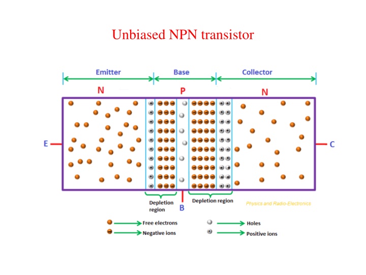
Bipolar Junction Transistor Common Base Configuration In this configuration, emitter is the input terminal, collector is the output terminal and base terminal is connected as a common terminal for both input and output. It is also known as grounded base configuration. The base-emitter junction JEis always forward biased and collector- base junction JCis always reverse biased. Let us consider NPN transistor in common base configuration.
Bipolar Junction Transistor Common Base Configuration The NPN transistor is formed when a single p-type semiconductor layer is sandwiched between two n-type semiconductor layers. Base-emitter junction JEis forward biased by the supply voltage VBEwhile the collector-base junction JCis reverse biased by the supply voltage VCB. Due to the forward bias voltage VBE, the free electronics (majority carriers) in the emitter region experience a repulsive force Similarly holes (majority carriers) in the base region experience a repulsive force
Bipolar Junction Transistor Common Base Configuration As a result, free electrons start flowing from emitter to base similarly holes start flowing from base to emitter. Thus free electrons which are flowing from emitter to base and holes which are flowing from base to emitter conducts electric current. The free electrons which are flowing from emitter to base will combine with the holes in the base region similarly the holes which are flowing from base to emitter will combine with the electrons in the emitter region. From the below figure, it is seen that the width of the base region is very thin. Therefore, only a small percentage of free electrons from emitter region will combine with the holes in the base region and the remaining large number of free electrons cross the base region and enters into the collector region.
Bipolar Junction Transistor Common Base Configuration A large number of free electrons which entered into the collector region will experience an attractive force from the positive terminal of the battery. Therefore, the free electrons in the collector region will flow towards the positive terminal of the battery. Thus, electric current is produced in the collector region.
Bipolar Junction Transistor Common Base Configuration The electric current produced at the collector region is primarily due to the free electrons from the emitter region similarly the electric current produced at the base region is also primarily due to the free electrons from emitter region. Therefore, the emitter current is greater than the base current and collector current. The emitter current is the sum of base current and collector current. IE= IB+ IC The output collector current is less than the input emitter current, so the current gain of this amplifier is actually less than 1. The base-emitter junction JEat input side acts as a forward biased diode. So the common base amplifier has a low input impedance (low opposition to incoming current)
Bipolar Junction Transistor Common Base Configuration The collector-base junction JCat output side acts somewhat like a reverse biased diode. So the common base amplifier has high output impedance. The common base amplifier provides a low input impedance and high output impedance. Transistors with low input impedance and high output impedance provide a high voltage gain. Even though the voltage gain is high, the current gain is very low and the overall power gain of the common base amplifier is low as compared to the other transistor amplifier configurations. The common base amplifier is mainly used as a voltage amplifier or current buffer. This type of transistor arrangement is not very common and is not as widely used as the other two transistor configurations.
Bipolar Junction Transistor Common Base Configuration-Working To fully describe the behaviour of a transistor with CB configuration, we need two set of characteristics: they are Input characteristics Input characteristics The input characteristics describe the relationship between input current (IE) and the input voltage (VBE). Output characteristics. To determine the input characteristics, the output voltage VCB(collector-base voltage) is kept constant at zero volts and the input voltage VBEis increased from zero volts to different voltage levels. For each voltage level of the input voltage (VBE), the input current (IE) is recorded
Bipolar Junction Transistor Common Base Configuration-Working -Input characteristics Next, the output voltage (VCB) is increased from zero volts to a certain voltage level (8 volts) and kept constant at 8 volts. While increasing the output voltage (VCB), the input voltage (VBE) is kept constant at zero volts. After we kept the output voltage (VCB) constant at 8 volts, the input voltage VBEis increased from zero volts to different voltage levels. For each voltage level of the input voltage (VBE), the input current (IE) is recorded A curve is then drawn between input current IEand input voltage VBEat constant output voltage VCB(8 volts). This is repeated for higher fixed values of the output voltage (VCB). When output voltage (VCB) is at zero volts and emitter-base junction JEis forward biased by the input voltage (VBE), the emitter-base junction acts like a normal p-n junction diode. So the input characteristics are same as the forward characteristics of a normal pn junction diode.
Bipolar Junction Transistor Common Base Configuration-Working -Input characteristics When the output voltage (VCB) is increased from zero volts to a certain voltage level (8 volts), the emitter current flow will be increased which in turn reduces the depletion region width at emitter-base junction. As a result, the cut in voltage will be reduced. Therefore, the curves shifted towards the left side for higher values of output voltage VCB.
Bipolar Junction Transistor Common Base Configuration-Working -Output characteristics The output characteristics describe the relationship between output current (IC) and the output voltage (VCB). To determine the output characteristics, the input current or emitter current IEis kept constant at zero mA and the output voltage VCBis increased from zero volts to different voltage levels. For each voltage level of the output voltage VCB, the output current (IC) is recorded. A curve is then drawn between output current ICand output voltage VCBat constant input current IE(0 mA). When the emitter current or input current IEis equal to 0 mA, the transistor operates in the cut-off region. Next, the input current (IE) is increased from 0 mA to 1 mA by adjusting the input voltage VBEand the input current IEis kept constant at 1 mA. While increasing the input current IE, the output voltage VCBis kept constant.
Bipolar Junction Transistor Common Base Configuration-Working -Output characteristics After we kept the input current (IE) constant at 1 mA, the output voltage (VCB) is increased from zero volts to different voltage levels. For each voltage level of the output voltage (VCB), the output current (IC) is recorded. A curve is then drawn between output current ICand output voltage VCBat constant input current IE(1 mA). This region is known as the active region of a transistor. This is repeated for higher fixed values of input current IE(I.e. 2 mA, 3 mA, 4 mA ) From the characteristics, we can see that for a constant input current IE, when the output voltage VCBis increased, the output current ICremains constant.
Bipolar Junction Transistor Common Base Configuration-Working -Output characteristics At saturation region, both emitter-base junction JEand collector-base junction JCare forward biased. From the above graph, we can see that a sudden increase in the collector current when the output voltage VCBmakes the collector-base junction JCforward biased. Early effect Due to forward bias, the base-emitter junction JEacts as a forward biased diode and due to reverse bias, the collector-base junction JCacts as a reverse biased diode. Therefore, the width of the depletion region at the base-emitter junction JEis very small whereas the width of the depletion region at the collector- base junction JCis very large. If the output voltage VCBapplied to the collector-base junction JCis further increased, the depletion region width further increases. The base region is lightly doped as compared to the collector region. So the depletion region penetrates more into the base region and less into the collector region. As a result, the width of the base region decreases. This dependency of base width on the output voltage (VCB) is known as an early effect.
Bipolar Junction Transistor Common Base Configuration-Transistor parameters Dynamic input resistance (ri) Dynamic input resistance is defined as the ratio of change in input voltage or emitter voltage (VBE) to the corresponding change in input current or emitter current (IE), with the output voltage or collector voltage (VCB) kept at constant. The input resistance of common base amplifier is very low. Dynamic output resistance (ro) Dynamic output resistance is defined as the ratio of change in output voltage or collector voltage (VCB) to the corresponding change in output current or collector current (IC), with the input current or emitter current (IE) kept at constant. The output resistance of common base amplifier is very high.
Bipolar Junction Transistor Common Base Configuration-Transistor parameters Current gain ( ) The current gain of a transistor in CB configuration is defined as the ratio of output current or collector current (IC) to the input current or emitter current (IE). The current gain of a transistor in CB configuration is less than unity. The typical current gain of a common base amplifier is 0.98.
Bipolar Junction Transistor Common Emitter Configuration In common emitter configuration, base is the input terminal, collector is the output terminal and emitter is the common terminal for both input and output. That means the base terminal and common emitter terminal are known as input terminals whereas collector terminal and common emitter terminal are known as output terminals. In common emitter configuration, the emitter terminal is grounded so the common emitter configuration is also known as grounded emitter configuration. The common emitter (CE) configuration is the most widely used transistor configuration. The common emitter (CE) amplifiers are used when large current gain is needed.
Bipolar Junction Transistor Common Emitter Configuration The input signal is applied between the base and emitter terminals while the output signal is taken between the collector and emitter terminals. Thus, the emitter terminal of a transistor is common for both input and output and hence it is named as common emitter configuration. The supply voltage & current between base and emitter is denoted by VBE& IBwhile the supply voltage& current between collector and emitter is denoted by VCE& IC. The common emitter amplifier has medium input and output impedance levels.
Bipolar Junction Transistor Common Emitter Configuration-Working To fully describe the behaviour of a transistor with CE configuration, we need two set of characteristics: they are Input characteristics Input characteristics The input characteristics describe the relationship between input current or base current (IB) and input voltage or base-emitter voltage (VBE). To determine the input characteristics, the output voltage VCEis kept constant at zero volts and the input voltage VBEis increased from zero volts to different voltage levels. For each voltage level of input voltage (VBE), the corresponding input current (IB) is recorded. A curve is then drawn between input current IBand input voltage VBEat constant output voltage VCE(0 volts). Next, the output voltage (VCE) is increased from zero volts to certain voltage level (10 volts) and the output voltage (VCE) is kept constant at 10 volts. Output characteristics.
Bipolar Junction Transistor Common Emitter Configuration-Input characteristics While increasing the output voltage (VCE), the input voltage (VBE) is kept constant at zero volts. After we kept the output voltage (VCE) constant at 10 volts, the input voltage VBEis increased from zero volts to different voltage levels. For each voltage the corresponding input current (IB) is recorded. A curve is then drawn between input current IBand input voltage VBEat constant output voltage VCE(10 volts). This process is repeated for higher fixed values of output voltage (VCE). When output voltage (VCE) is at zero volts and emitter-base junction is forward biased by input voltage (VBE), the emitter-base junction acts like a normal p-n junction diode. So the input characteristics of the CE configuration is same as the characteristics of a normal pn junction diode. level of input voltage (VBE),
Bipolar Junction Transistor Common Emitter Configuration-Input characteristics In common emitter (CE) configuration, the input current (IB) is very small as compared to the input current configuration. The input current in CE configuration is measured in microamperes ( A) whereas the input current in CB configuration is measured in milliamperes (mA). In common emitter (CE) configuration, the input current (IB) is produced in the base region which is lightly doped and has small width. So the base region produces only a small input current (IB). On the other hand, in common base (CB) configuration, the input current (IE) is produced in the emitter region which is heavily doped and has large width. So the emitter region produces a large input current (IE). Therefore, the input current (IB) produced in the common emitter (CE) configuration is small as compared to the common base (CB) configuration. Due to forward bias, the emitter-base junction acts as a forward biased diode and due to reverse bias, the collector-base junction acts as a reverse biased diode. (IE) in common base (CB)
Bipolar Junction Transistor Common Emitter Configuration-Input characteristics Therefore, the width of the depletion region at the emitter-base junction is very small whereas the width of the depletion region at the collector-base junction is very large. If the output voltage VCEapplied to the collector-base junction is further increased, the depletion region width further increases. The base region is lightly doped as compared to the collector region. So the depletion region penetrates more into the base region and less into the collector region. As a result, the width of the base region decreases which in turn reduces the input current (IB) produced in the base region. From the above characteristics, we can see that for higher fixed values of output voltage VCE, the curve shifts to the right side. This is because for higher fixed values of output voltage, the cut in voltage is increased above 0.7 volts. Therefore, to overcome this cut in voltage, more input voltage VBEis needed than previous case.
Bipolar Junction Transistor Common Emitter Configuration- Output characteristics Output characteristics The output characteristics describe the relationship between output current (IC) and output voltage (VCE). To determine the output characteristics, the input current or base current IBis kept constant at 0 A and the output voltage VCEis increased from zero volts to different voltage levels. For each level of output voltage, the corresponding output current (IC) is recorded. A curve is then drawn between output current ICand output voltage VCEat constant input current IB(0 A). When the base current or input current IB= 0 A, the transistor operates in the cut-off region. In this region, both junctions are reverse biased. Next, the input current (IB) is increased from 0 Ato 20 Aby adjusting the input voltage (VBE). The input current (IB)is kept constant at 20 A.
Bipolar Junction Transistor Common Emitter Configuration- Output characteristics Output characteristics After we kept the input current (IB) constant at 20 A, the output voltage (VCE) is increased from zero volts to different voltage levels. For each voltage level of output voltage (VCE), the corresponding output current (IC) is recorded. A curve is then drawn between output current ICand output voltage VCEat constant input current IB(20 A). This region is known as the active region of a transistor. In this region, emitter-base junction is forward biased and the collector-base junction is reverse biased. This steps are repeated for higher fixed values of input current IB(I.e. 40 A, 60 A, 80 Aand so on).
Bipolar Junction Transistor Common Emitter Configuration- Output characteristics Output characteristics When output voltage VCEis reduced to a small value (0.2 V), the collector-base junction becomes forward biased. This is because the output voltage VCEhas less effect on collector-base junction than input voltage VBE. As we know that the emitter-base junction is already forward biased. therefore, when both the junctions are forward biased, the transistor operates in the saturation region. In this region, a small increase in output voltage VCEwill rapidly increases the output current IC.
Bipolar Junction Transistor Common Emitter Configuration- Transistor parameters Dynamic input resistance (ri) Dynamic input resistance is defined as the ratio of change in input voltage or base voltage (VBE) to the corresponding change in input current or base current (IB), with the output voltage or collector voltage (VCE) kept at constant. In CE configuration, the output resistance is high.Current gain ( ) The current gain of a transistor in CE configuration is defined as the ratio of output current or collector current (IC) to the input current or base current (IB). The current gain of a transistor in CE configuration is high. Therefore, the transistor in CE configuration is used for amplifying the current.
Bipolar Junction Transistor Common Collector Configuration In this configuration, the base terminal of the transistor serves as the input, the emitter terminal is the output and the collector terminal is common for both input and output. Hence, it is named as common collector configuration. The input is applied between the base and collector while the output is taken from the emitter and collector. The common collector configuration is also referred to as emitter follower, voltage follower, common collector amplifier, CC amplifier, or CC configuration. This configuration is mostly used as a voltage buffer. The input supply voltage between base and collector is denoted by VBCwhile the output voltage between emitter and collector is denoted by VEC.
Bipolar Junction Transistor Common Collector Configuration In this configuration, input current or base current is denoted by IBand output current or emitter current is denoted by IE. The common collector amplifier has high input impedance and low output impedance. It has low voltage gain and high current gain. The power gain of the common collector amplifier is medium. To fully describe the behaviour of a transistor with CC configuration, we need two set of characteristics - input characteristics and output characteristics.
Bipolar Junction Transistor Common Collector Configuration-Working To fully describe the behaviour of a transistor with CC configuration, we need two set of characteristics: they are Input characteristics Input characteristics The input characteristics describe the relationship between input current or base current (IB) and input voltage or base-collector voltage (VBC). Output characteristics. To determine the input characteristics, the output voltage VECis kept constant at 3V and the input voltage VBCis increased from zero volts to different voltage levels. For each level of input voltage VBC, the corresponding input current IBis noted. A curve is then drawn between input current IBand input voltage VBCat constant output voltage VEC(3V).
Bipolar Junction Transistor Common Collector Configuration- Input characteristics Next, the output voltage VECis increased from 3V to different voltage level, say for example 5V and then kept constant at 5V. While increasing the output voltage VEC, the input voltage VBCis kept constant at zero volts. After we kept the output voltage VECconstant at 5V, the input voltage VBCis increased from zero volts to different voltage levels. For each level of input voltage VBC, the corresponding input current IBis noted. A curve is then drawn between input current IBand input voltage VBCat constant output voltage VEC(5V). This process is repeated for higher fixed values of output voltage (VEC).
Bipolar Junction Transistor Common Collector Configuration- Output characteristics Output characteristics The output characteristics describe the relationship between output current or emitter current (IE) and output voltage or emitter-collector voltage(VEC). To determine the output characteristics, the input current IBis kept constant at zero micro amperes and the output voltage VECis increased from zero volts to different voltage levels. For each level of output voltage VEC, the corresponding output current IEis noted. A curve is then drawn between output current IEand output voltage VECat constant input current IB(0 A). Next, the input current (IB) is increased from 0 A to 20 A and then kept constant at 20 A. While increasing the input current (IB), the output voltage (VEC) is kept constant at 0 volts.
Bipolar Junction Transistor Common Collector Configuration- Output characteristics Output characteristics After we kept the input current (IB) constant at 20 A, the output voltage (VEC) is increased from zero volts to different voltage levels. For each level of output voltage (VEC), the corresponding output current (IE) is recorded. A curve is then drawn between output current IE and output voltage VECat constant input current IB(20 A). This region is known as the active region of a transistor. This process is repeated for higher fixed values of input current IB(I.e. 40 A, 60 A, 80 Aand so on).
Bipolar Junction Transistor Common Collector Configuration- Output characteristics Output characteristics In common collector configuration, if the input current or base current is zero then the output current or emitter current is also zero. As a result, no current flows through the transistor. So the transistor will be in the cut-off region. If the base current is slightly increased then the output current or emitter current also increases. So the transistor falls into the active region. If the base current is heavily increased then the current flowing through the transistor also heavily increases. As a result, the transistor falls into the saturation region.
Bipolar Junction Transistor Common Collector Configuration- Transistor parameters Dynamic input resistance (ri) Dynamic input resistance is defined as the ratio of change in input voltage or base voltage (VBC) to the corresponding change in input current or base current (IB), with the output voltage or emitter voltage (VEC) kept at constant. The input resistance of common collector amplifier is high. Current amplification factor ( ) The current amplification factor is defined as the ratio of change in output current or emitter current IE to the change in input current or base current IB. It is expressed by . The current gain of a common collector amplifier is high.