Digital System Fundamentals: Complex FSMs in Sequential Circuits
This content discusses complex Finite State Machines (FSMs) in sequential circuits, focusing on performing register operations and counting divisions. It explains the inputs, outputs, transition conditions, and the role of registers in achieving specific tasks within the circuit.

Download Presentation

Please find below an Image/Link to download the presentation.
The content on the website is provided AS IS for your information and personal use only. It may not be sold, licensed, or shared on other websites without obtaining consent from the author.If you encounter any issues during the download, it is possible that the publisher has removed the file from their server.
You are allowed to download the files provided on this website for personal or commercial use, subject to the condition that they are used lawfully. All files are the property of their respective owners.
The content on the website is provided AS IS for your information and personal use only. It may not be sold, licensed, or shared on other websites without obtaining consent from the author.
E N D
Presentation Transcript
ECE 352 Digital System Fundamentals Complex FSMs Complex FSMs 1 1
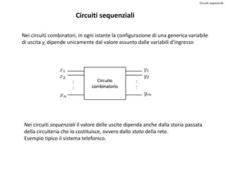
Example Complex FSM This is a sequential circuit that performs a series of register operations Transition conditions may be based on input signals or register values Inputs: START / Q 0 R InA D InB Complex FSMs START InA InB Outputs: V Q R (R D) > 0? / R R D Q Q + 1 D D START INIT SUB Some outputs may be register outputs; some inputs may be buses (R D) == 0? / R R D Q Q + 1 D D (R D) < 0? / R R Q Q D D reset DONE In this type of diagram, we assume registers hold if no operation is given R Q D R Q D Mix of V Mealy/Moore 2 2
Example Complex FSM What does this do? DIVISION Counts the number of times it can subtract the InB from InA without going negative START / Q 0 R InA D InB Complex FSMs (R D) > 0? / R R D Q Q + 1 START Sets output V = 1 for one cycle when it is finished INIT SUB (R D) == 0? / R R D Q Q + 1 (R D) < 0? reset DONE V 3 3
Breaking Down a Problem What are the circuit inputs? InA and InB are vector inputs (multi-bit busses) that are the operands for the division START is a scalar signal that tells the circuit to begin processing START / Q 0 R InA D InB Complex FSMs (R D) > 0? / R R D Q Q + 1 START INIT SUB (R D) == 0? / R R D Q Q + 1 (R D) < 0? reset DONE Inputs: START InA InB Outputs: V Q R V 4 4
Breaking Down a Problem What are the circuit outputs? The data outputs of registers R and Q are the results of the division: Q: quotient R: remainder START / Q 0 R InA D InB Complex FSMs (R D) > 0? / R R D Q Q + 1 START INIT SUB (R D) == 0? / R R D Q Q + 1 V indicates if the operation is complete (R D) < 0? reset DONE Inputs: START InA InB Outputs: V Q R V 5 5
Breaking Down a Problem What are the registers and their capabilities? Register D: D InB Load D D Hold START / Q 0 R InA D InB Complex FSMs (R D) > 0? / R R D Q Q + 1 D D START INIT SUB (R D) == 0? / R R D Q Q + 1 D D (R D) < 0? / D D reset Don t forget implied hold behavior DONE / D D V 6 6
Breaking Down a Problem What are the registers and their capabilities? Register D: D InB Load D D Hold START / Q 0 R InA D InB Complex FSMs (R D) > 0? / R R D Q Q + 1 START Register R: R InA R R D Subtract R R Load INIT SUB Hold (R D) == 0? / R R D Q Q + 1 (R D) < 0? / R R reset DONE / R R V 7 7
Breaking Down a Problem What are the registers and their capabilities? Register D: D InB Load D D Hold START / Q 0 R InA D InB Complex FSMs (R D) > 0? / R R D Q Q + 1 START Register R: R InA R R D Subtract R R Load INIT SUB Hold (R D) == 0? / R R D Q Q + 1 (R D) < 0? / Q Q Register Q: Q 0 Q Q + 1 Increment Q Q reset Sync. Clear DONE / Q Q V Hold 8 8
Breaking Down a Problem What are the registers and their capabilities? Register D: D InB Load D D Hold START / Q 0 R InA D InB Complex FSMs (R D) > 0? / R R D Q Q + 1 START Register R: R InA R R D Subtract R R Load INIT SUB Hold (R D) == 0? / R R D Q Q + 1 (R D) < 0? Register Q: Q 0 Q Q + 1 Increment Q Q reset Sync. Clear DONE V Hold 9 9
Breaking Down a Problem What are the control signals? Register D: D InB Load D D Hold loadD 1 0 We are designing the entire circuit, so we can choose what happens if multiple register control inputs are 1 Complex FSMs Register R: R InA R R D Subtract R R loadR subR 1 0 0 Load 0 1 0 Hold 1 1 Undefined Register Q: Q 0 Q Q + 1 Increment Q Q Undefined clrQ 1 0 0 1 incQ 0 1 0 1 Sync. Clear Hold 10 10
Breaking Down a Problem What status information does the control FSM need from the datapath? Status Flag RgtD RltD ReqD Condition START / Q 0 R InA D InB Complex FSMs (R D) > 0? / R R D Q Q + 1 START (R D) > 0? (R D) < 0? (R D) == 0? INIT SUB (R D) == 0? / R R D Q Q + 1 (R D) < 0? reset DONE V 11 11
Breaking Down a Problem Datapath: Register R with inputs InA, loadR and subR Register D with inputs InB and loadD Register Q with inputs clrQ and incQ Subtractor (R D) with outputs RgtD, RltD, ReqD Circuit outputs Q and R Control FSM: Inputs RgtD, RltD, ReqD from the datapath Input START (circuit input) Outputs clrQ, loadR, loadD, incQ, subR Circuit outputV Three states (INIT, SUB, DONE) Complex FSMs 12 12
Define the Interface Datapath and control need to communicate Some datapath inputs are control outputs Some control inputs are datapath outputs START Complex FSMs Datapath Control START loadR subR loadD clrQ incQ RgtD RltD ReqD V V InA InB InA[n..0] loadR subR loadD clrQ incQ RgtD RltD ReqD Notice that the control unit never knows either of the operands or the result! InB[n..0] CLK R Q CLK RST CLK RST R[n..0] Q[n..0] 13 13
Next Steps Design each component (datapath and control) based on the defined interface between them Create registers that respond correctly to the defined control signals Create an FSM that generates the needed control signal values at the needed times Complex FSMs Now that we have defined the interface, the design of the components is independent We can design them in either order 14 14
Design the Datapath Design the registers based on the specific behavior, control signals, and status outputs Datapath Control START loadR subR loadD clrQ incQ RgtD RltD ReqD Complex FSMs V START V InA D loadR subR RgtD RltD ReqD Reg R InA[n..0] CLK R Reg D D InB CLK InB[n..0] loadD CLK RST Reg Q Q clrQ incQ CLK R[n..0] Q[n..0] CLK RST 15 15
Design the Control Redraw the complex FSM in terms of the newly- defined interface between datapath and control Replace register condition tests with datapath status outputs (which are inputs to the control FSM) Replace register transfer operations with datapath control inputs (outputs of the control FSM) Complex FSMs 16 16
Design the Control Replace register condition tests with datapath status outputs (inputs to the control FSM) START / Q 0 R InA D InB Complex FSMs RgtD / (R D) > 0? / R R D Q Q + 1 START INIT SUB ReqD / (R D) == 0? / R R D Q Q + 1 (R D) < 0? RltD / reset DONE Inputs: START RgtD Outputs: V RltD ReqD V 17 17
Design the Control Replace register transfer operations with datapath control inputs (outputs of the control FSM) START / Q 0 R InA D InB loadD Complex FSMs RgtD / (R D) > 0? / R R D Q Q + 1 incQ clrQ START subR loadR INIT SUB ReqD / (R D) == 0? / R R D Q Q + 1 incQ (R D) < 0? RltD / subR reset DONE RgtD RltD ReqD Inputs: START Outputs: V V loadD clrQ loadR subR incQ 18 18
Design the Control Create FSM logic using either minimum-FF or one-hot design method = QDONE + START QINIT DINIT (one-hot shown here) DSUB = START QINIT + RgtD QSUB START / Q 0 R InA D InB loadD Complex FSMs RgtD / subR (R D) > 0? / R R D Q Q + 1 incQ clrQ START DDONE = (RltD + ReqD) QSUB loadR clrQ = loadR = loadD = INIT SUB START QINIT subR = incQ = ReqD / subR (R D) == 0? / R R D Q Q + 1 incQ (R D) < 0? RltD / (RgtD + ReqD) QSUB = QDONE V reset DONE Inputs: START Outputs: V RgtD RltD ReqD V loadD clrQ loadR subR incQ 19 19
Design the Control Notice that there really are only two datapath control signals (the others are redundant)! = QDONE + START QINIT DINIT DSUB = START QINIT + RgtD QSUB START / Q 0 R InA D InB loadD Complex FSMs RgtD / subR (R D) > 0? / R R D Q Q + 1 incQ clrQ START DDONE = (RltD + ReqD) QSUB loadR clrQ = loadR = loadD = INIT SUB START QINIT subR = incQ = ReqD / subR (R D) == 0? / R R D Q Q + 1 incQ (R D) < 0? RltD / (RgtD + ReqD) QSUB = QDONE V reset DONE Inputs: START Outputs: V RgtD RltD ReqD V loadD clrQ loadR subR incQ 20 20
Block Diagram Revisited Once the datapath and control are created, they can be combined to form the complete circuit Datapath Control START loadR subR loadD clrQ incQ RgtD RltD ReqD Complex FSMs V START V InA D loadR subR RgtD RltD ReqD Reg R InA[n..0] CLK R Reg D D InB CLK InB[n..0] loadD CLK RST Reg Q Q clrQ incQ CLK R[n..0] Q[n..0] CLK RST 21 21
How Does The Timing Work? START InA InB 17 13 27 5 Until a reset, we do not know what state we are in! RST CLK Q R D RgtD RltD ReqD 0 1 2 7 START 3 2 0 START / Q 0 R InA D InB loadD Complex FSMs RgtD / subR 17 5 12 13 27 (R D) > 0? / R R D Q Q + 1 incQ clrQ loadR INIT SUB State Next clrQ subR INIT DONE INIT SUB SUB ReqD / subR INIT SUB INIT (R D) < 0? RltD / (R D) == 0? / R R D Q Q + 1 incQ DONE SUB DONE reset V DONE Inputs: START Outputs: V RgtD RltD ReqD V loadD clrQ loadR subR incQ 22 22
How Does The Timing Work? START A reset puts the FSM into the INIT state, but does not affect the datapath registers InA InB 17 13 27 5 RST CLK Q R D RgtD RltD ReqD 0 1 2 7 START 3 2 0 START / Q 0 R InA D InB loadD Complex FSMs RgtD / subR 17 5 12 13 27 (R D) > 0? / R R D Q Q + 1 incQ clrQ loadR INIT SUB State Next clrQ subR INIT DONE INIT SUB SUB ReqD / subR INIT SUB INIT (R D) < 0? RltD / (R D) == 0? / R R D Q Q + 1 incQ DONE SUB DONE reset V DONE Inputs: START Outputs: V RgtD RltD ReqD V loadD clrQ loadR subR incQ 23 23
How Does The Timing Work? START The datapath registers have not yet updated in response to clrQ InA InB 17 13 27 5 RST CLK Q R D RgtD RltD ReqD 0 1 2 7 START 3 2 0 START / Q 0 R InA D InB loadD Complex FSMs RgtD / subR 17 5 12 13 27 (R D) > 0? / R R D Q Q + 1 incQ clrQ loadR INIT SUB State Next clrQ subR INIT DONE INIT SUB SUB ReqD / subR INIT SUB INIT (R D) < 0? RltD / (R D) == 0? / R R D Q Q + 1 incQ DONE SUB DONE reset V DONE Inputs: START Outputs: V RgtD RltD ReqD V loadD clrQ loadR subR incQ 24 24
How Does The Timing Work? START Datapath registers update at the InA InB 17 13 27 active clock edge based on control signal values just before the edge! 5 RST CLK Q R D RgtD RltD ReqD 0 1 2 7 START 3 2 0 START / Q 0 R InA D InB loadD Complex FSMs RgtD / subR 17 5 12 13 27 (R D) > 0? / R R D Q Q + 1 incQ clrQ loadR INIT SUB State Next clrQ subR INIT DONE INIT SUB SUB ReqD / subR INIT SUB INIT (R D) < 0? RltD / (R D) == 0? / R R D Q Q + 1 incQ DONE SUB DONE reset V DONE Inputs: START Outputs: V RgtD RltD ReqD V loadD clrQ loadR subR incQ 25 25
How Does The Timing Work? START InA InB 17 13 27 5 RST CLK Q R D RgtD RltD ReqD 0 1 2 7 START 3 2 0 START / Q 0 R InA D InB loadD Complex FSMs RgtD / subR 17 5 12 13 27 (R D) > 0? / R R D Q Q + 1 incQ clrQ loadR INIT SUB State Next clrQ subR INIT DONE INIT SUB SUB ReqD / subR INIT SUB INIT (R D) < 0? RltD / (R D) == 0? / R R D Q Q + 1 incQ DONE SUB DONE reset V DONE Inputs: START Outputs: V RgtD RltD ReqD V loadD clrQ loadR subR incQ 26 26
How Does The Timing Work? START / Q 0 R InA D InB loadD START (R D) > 0? / R R D Q Q + 1 incQ RgtD / subR clrQ START InA InB 17 13 27 loadR 5 INIT SUB RST CLK Q R D RgtD RltD ReqD (R D) == 0? / R R D Q Q + 1 incQ (R D) < 0? RltD / ReqD / subR 0 1 2 7 3 2 0 Complex FSMs reset 17 5 12 13 27 DONE V State Next clrQ subR INIT DONE INIT SUB SUB INIT SUB INIT DONE SUB DONE Keep subtracting until R is less than or equal to D V 27 27
How Does The Timing Work? START / Q 0 R InA D InB loadD START (R D) > 0? / R R D Q Q + 1 incQ RgtD / subR clrQ START InA InB 17 13 27 loadR 5 INIT SUB RST CLK Q R D RgtD RltD ReqD (R D) == 0? / R R D Q Q + 1 incQ (R D) < 0? RltD / ReqD / subR 0 1 2 7 3 2 0 Complex FSMs reset 17 5 12 13 27 DONE V State Next clrQ subR INIT DONE INIT SUB SUB INIT SUB INIT DONE SUB DONE Now R is less than D, so the division is complete V 28 28
How Does The Timing Work? START InA InB 17 13 27 5 RST CLK Q R D RgtD RltD ReqD 0 1 2 7 3 2 0 Assert V to indicate that the Q and R values are the (valid) final result Complex FSMs 17 5 12 13 27 State Next clrQ subR INIT DONE INIT SUB SUB INIT SUB INIT DONE SUB DONE V 29 29
How Does The Timing Work? START / Q 0 R InA D InB loadD Complex FSMs RgtD / subR After the operation completes, unconditionally transition back to the INIT state (R D) > 0? / R R D Q Q + 1 incQ clrQ START loadR INIT SUB ReqD / subR (R D) == 0? / R R D Q Q + 1 incQ (R D) < 0? RltD / reset DONE Inputs: START Outputs: V RgtD RltD ReqD V loadD clrQ loadR subR incQ 30 30
How Does The Timing Work? START InA InB 17 13 27 Begin a new operation 5 RST CLK Q R D RgtD RltD ReqD 0 1 2 7 3 2 0 Complex FSMs 17 5 12 13 27 State Next clrQ subR INIT DONE INIT SUB SUB INIT SUB INIT DONE SUB DONE V 31 31
How Does The Timing Work? Begin a new operation START / Q 0 R InA D InB loadD Complex FSMs RgtD / subR (R D) > 0? / R R D Q Q + 1 incQ clrQ START loadR INIT SUB ReqD / subR (R D) == 0? / R R D Q Q + 1 incQ (R D) < 0? RltD / reset DONE Inputs: START Outputs: V RgtD RltD ReqD V loadD clrQ loadR subR incQ 32 32
How Does The Timing Work? START InA InB 17 13 27 5 RST CLK Q R D RgtD RltD ReqD 0 1 2 7 3 2 0 Complex FSMs 17 5 12 13 27 State Next clrQ subR INIT DONE INIT SUB SUB INIT SUB INIT DONE SUB DONE V What happens here? 33 33
Analyzing the Complex FSM 1. What happens when InA < InB? 2. What happens when InA == InB? 3. What happens if InB == 0? 4. Does this work for signed numbers? 5. What is its max throughput (relative to fMAX)? Complex FSMs START / Q 0 R InA D InB (R D) > 0? / R R D Q Q + 1 START INIT SUB (R D) == 0? / R R D Q Q + 1 (R D) < 0? reset DONE V 34 34
Analyzing the Complex FSM 1. It goes directly from INIT to SUB to DONE, without doing a subtraction operation, so the answer will (correctly) be reported as 0 remainder InA. 2. It goes directly from INIT to SUB to DONE, doing a single subtraction operation so the answer will (correctly) be reported as 1 remainder 0. 3. If InA is not also equal to 0, the machine is stuck in state SUB forever! If InA is 0, it (incorrectly) reports the result as 1 remainder 0! 4. Not in general. It was designed for positive numbers, so it will not properly handle all combinations of positive and negative operands. 5. Max throughput is fMAX/3, since every division operation requires at least 3 clock cycles. Complex FSMs 35 35
ECE 352 Digital System Fundamentals Complex FSMs Complex FSMs 36 36