Use of Op-Amp as Comparator Circuits

Figure 17.3a demonstrates a circuit using an op-amp as a comparator with a positive reference voltage. An LED indicator is connected to show when the input voltage surpasses the reference level. Alternatively, Figure 17.4 depicts a voltage comparator circuit capable of operating from various power supplies and driving different loads. The use of a 311 IC in Figure 17.5 for zero-crossing detection and a 311 comparator with strobing in Figure 17.6 are also explained along with their functionalities.

Download Presentation

Please find below an Image/Link to download the presentation.
The content on the website is provided AS IS for your information and personal use only. It may not be sold, licensed, or shared on other websites without obtaining consent from the author.If you encounter any issues during the download, it is possible that the publisher has removed the file from their server.
You are allowed to download the files provided on this website for personal or commercial use, subject to the condition that they are used lawfully. All files are the property of their respective owners.
The content on the website is provided AS IS for your information and personal use only. It may not be sold, licensed, or shared on other websites without obtaining consent from the author.
E N D
Presentation Transcript
Use of Op-Amp as Comparator Figure 17.3a shows a circuit operating with a positive reference voltage connected to the minus input and the output connected to an indicator LED. The reference voltage level is set at Since the reference voltage is connected to the inverting input, the output will switch to its positive saturation level when the input, Vi, goes more positive than the 6-V reference voltage level. The output, Vo, then drives the LED ON as an indication that the input is more positive than the reference level. in Fig. 17.3b shows As an alternative connection, the positive reference voltage could be connected to the noninverting input and input voltage will connected to inverting input for omp-amplifier that the output will switch to its positive saturation level when the input, Vi, goes less than the 6-V reference voltage level.
311 COMPARATOR Page 723
311 voltage comparator shown in Fig. 17.4 contains a comparator circuit that can operate as well from dual power supplies of 15 V as from a single 5-V supply. The output can provide a voltage at one of two distinct levels or can be used to drive a lamp or a relay. The output is taken from a bipolar transistor to allow driving a variety of loads.
A zero-crossing detector that senses (detects) the input voltage crossing through 0 V is shown using the 311 IC in Fig. 17.5. The inverting input is connected to ground (the reference voltage). The input signal going positive drives the output transistor ON, with the output then going low (-10 V in this case). The input signal going negative (below 0 V) will drive the output transistor OFF, the output then going high (to +10 V). The output is thus an indication of whether the input is above or below 0 V.
When the input is any positive voltage, the output is low, while any negative voltage will result in the output going to a high voltage level.
311 comparator with strobing Figure 17.6 shows how a 311 comparator can be used with strobing. In this example, the output will go high when the input goes above the reference level but only if the TTL strobe input is off (or 0 V). If the TTL strobe input goes high, it drives the 311 strobe input at pin 6 low, causing the output to remain in the off state (with output high) regardless of the input signal. In effect, the output remains high unless strobed. If strobed, the output then acts normally, switching from high to low depending on the input signal level. In operation, the comparator output will respond to the input signal only during the time the strobe signal allows such operation.
311 comparator output driving a relay. Figure 17.7 shows the comparator output driving a relay. When the input goes below 0 V, driving the output low, the relay is activated, closing the normally open (N.O.) contacts at that time. These contacts can then be connected to operate a large variety of devices. For example, a buzzer or bell wired to the contacts can be driven on whenever the input voltage drops below 0 V. As long as the voltage is present at the input terminal, the buzzer will remain off.
339 COMPARATOR The 339 IC is a quad comparator containing four independent voltage comparator circuits connected to external pins as shown in Fig. 17.8. Each comparator has inverting and noninverting inputs and a single output. The supply voltage applied to a pair of pins powers all four comparators. Even if one wishes to use one comparator, all four will be drawing power.
339 COMPARATOR To see how these comparator circuits can be used, Fig. 17.9 shows one of the 339 comparator circuits connected as a zero-crossing detector. Whenever the input signal goes above 0 V, the output switches to V+. The input switches to V- only when the input goes below 0 V. A reference level other than 0 V can also be used, and either input terminal could be used as the reference, the other terminal then being connected to the input signal. The operation of one of the comparator circuits is described next.
The differential input voltage (difference voltage across input terminals) going positive drives the output transistor off (open circuit), while a negative differential input voltage drives the output transistor on the output then at the supply low level. If the negative input is set at a reference level Vref, the positive input goes above Vref and results in a positive differential input with output driven to the open-circuit state. When the noninverting input goes below Vref, resulting in a negative differential input, the output will be driven to V-. If the positive input is set at the reference level, the inverting input going below Vref results in the output open circuit while the inverting input going above Vref results in the output at V-. This operation is summarized in Fig. 17.10.
Since the output of one of these comparator circuits is from an open-circuit collector, applications in which the outputs from more than one circuit can be wire-ORed are possible. Figure 17.11 shows two comparator circuits connected with common output and also with common input. Comparator 1 has a +5 V reference voltage put connected to the noninverting input. The output will be driven low by comparator 1 when the input signal goes above +5 V. (Vin > +5) Comparator 2 has a reference voltage of +1 V connected to the inverting input. The output of comparator 2 will be driven low when the input signal goes below +1 V. (Vin<1) In total, the output will go low whenever the input is below +1 V or above +5 V, as shown in Fig. 17.11, the overall operation being that of a voltage window
DIGITALANALOG CONVERTERS Many voltages and currents in electronics vary continuously over some range of values. In digital circuitry the signals are at either one of two levels, representing the binary values of 1 or zero. An analog digital converter (ADC) obtains a digital value representing an input analog voltage. while a digital analog converter (DAC) changes a digital value back into an analog voltage.
Digital-to-Analog Conversion LADDER NETWORK CONVERSION One popular scheme uses a network of resistors, called a ladder network. A ladder network accepts inputs of binary values at, typically, 0 V or Vref and provides an output voltage proportional to the binary input value. Figure 17.12a shows a ladder network with four input voltages, representing 4 bits of digital data and a dc voltage output. The output voltage is proportional to the digital input value as given by the relation
Ladder network Therefore, (0110)2, digital, converts to 6 V, analog. The function of the ladder network is to convert the 16 possible binary values from 0000 to 1111 into one of 16 voltage levels in steps of Vref/16. Using more sections of ladder allows having more binary inputs and greater quantization for each step. For example, a 10-stage ladder network could extend the number of voltage steps or the voltage resolution to Vref/210 or Vref/1024. A reference voltage of Vref 10 V would then provide output voltage steps of 10 V/1024 or approximately 10 mV. Notes : More ladder stages provide greater voltage resolution. In general, the voltage resolution for n ladder stages is
ladder network Figure 17.13 shows a block diagram of a typical DAC using a ladder network. The ladder network, referred in the diagram as an R-2R ladder, is sandwiched between the reference current supply and current switches connected to each binary input, the resulting output current proportional to the input binary value. The binary input turns on selected legs of the ladder, the output current being a weighted summing of the reference current. Connecting the output current through a resistor will produce an analog voltage, if desired.
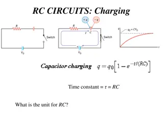
Analog-to-Digital Conversion DUAL-SLOPE CONVERSION A popular method for converting an analog voltage into a digital value is the dual slope method. Figure 17.14a shows a block diagram of the basic dual-slope converter. The analog voltage to be converted is applied through an electronic switch to an integrator or ramp-generator circuit (essentially a constant current charging a capacitor to produce a linear ramp voltage). The digital output is obtained from a counter operated during both positive and negative slope intervals of the integrator. The method of conversion proceeds as follows. For a fixed time interval (usually the full count range of the counter), the analog voltage connected to the integrator raises the voltage at the comparator input to some positive level.
Figure 17.14b shows that at the end of the fixed time interval the voltage from the integrator is greater for the larger input voltage. At the end of the fixed count interval, the count is set to zero and the electronic switch connects the integrator to a reference or fixed input voltage The integrator output (or capacitor input) then decreases at a fixed rate. The counter advances during this time, while the integrator s output decreases at a fixed rate until it drops below the comparator reference voltage, at which time the control logic receives a signal (the comparator output) to stop the count. The digital value stored in the counter is then the digital output of the converter
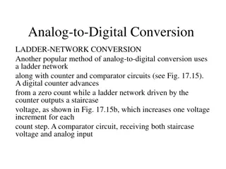
LADDER-NETWORK CONVERSION Another popular method of analog-to-digital conversion uses a ladder network along with counter and comparator circuits (see Fig. 17.15). A digital counter advances from a zero count while a ladder network driven by the counter outputs a staircase voltage, as shown in Fig. 17.15b, which increases one voltage increment for each count step. A comparator circuit, receiving both staircase voltage and analog input voltage, provides a signal to stop the count when the staircase voltage rises above the input voltage. The counter value at that time is the digital output.
The amount of voltage change stepped by the staircase signal depends on the number of count bits used. This would result in a conversion resolution of 2.4 mV. The clock rate of the counter would affect the time required to A 12-stage counter operating a 12-stage ladder network using a reference voltage of 10 V would step each count by a voltage of carry out a conversion. A clock rate of 1 MHz operating a 12-stage counter would need a maximum conversion time of


 the input")