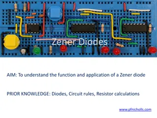
Zener and PIN Diodes
Zener diodes are designed to reliably conduct backwards at a set reverse voltage known as the Zener voltage. They have a well-defined reverse breakdown voltage and are used for voltage regulation. PIN diodes, with an intrinsic region between P-type and N-type semiconductors, are versatile in various applications like attenuators and photodetectors.

Uploaded on Mar 11, 2025 | 0 Views
Download Presentation

Please find below an Image/Link to download the presentation.
The content on the website is provided AS IS for your information and personal use only. It may not be sold, licensed, or shared on other websites without obtaining consent from the author.If you encounter any issues during the download, it is possible that the publisher has removed the file from their server.
You are allowed to download the files provided on this website for personal or commercial use, subject to the condition that they are used lawfully. All files are the property of their respective owners.
The content on the website is provided AS IS for your information and personal use only. It may not be sold, licensed, or shared on other websites without obtaining consent from the author.
E N D
Presentation Transcript
Dr.A.ANBARASI, ASSOCIATE PROFESSOR, DEPARTMENT OF PHYSICS, PERIYAR ARTS COLLEGE CUDDALORE
A of Zener diode current diode designed to is a special reliably backwards when a certain set reverse voltage is known as the Zener voltage is reached. Zener manufactured with a great variety of Zener voltages and some are even variable. type allow to flow ZENER DIODE ZENER DIODE * The diode consists of special heavily doped p-n junction * It is designed to conduct in the reverse direction when a certain specified voltage is reached. * Zener diode has a well-defined reverse- breakdown voltage at which starts conducting current. * And continue operating continuously in the reverse mode without damaged diode is
The voltage droACROSS THE DIODE REMAIN CONSTANT over a wide range of voltages. The Zener diode is suitable for use in voltage regulation.
ZENER DIODE OPERATION ZENER DIODE OPERATION The Zener diode operates like the normal diode when in the forward-bias mode And has turn-on voltage of 3.0 and 0.7V When connected to reverse mode which is mostly used in various applications (i.e. small leakage current flow). The current increases to a maximum, which is determined by the series resistor. After it is stabilizes remains constant over a wide range of applied voltages.
ZENER BREAKDOWN ZENER BREAKDOWN The breakdown due to Zener breakdown effect that occurs below 5.5V Each mechanisms has a different temperature co-efficient. The Zener effect has a negative temperature co-efficient while the impact of positive co-efficient. ZENER DIODE SPECIFICATION ZENER DIODE SPECIFICATION Such as normal working voltage, power dissipation, maximum reverse current.
PIN DIODES PIN DIODES A PIN diode is a diode with a wide undoped intrinsic semiconductor region between a P-type and N-type semiconductors region . P-type and N-type region are heavily doped because of their ohmic contacts Mostly used in attenuators, fast switches, photodetectors, and high voltage power electronics application.
PIN diodes also called high level injection. I region is flooded with charge carriers from the P region and N region For example, filling up the water bucket with a hole on the side. Electric field helps in speeding up of the transport of charge carriers from P side to N region. This device is used for high frequency operations.
CHARACTERISTICS OF PIN DIODE CHARACTERISTICS OF PIN DIODE PIN diode obeys the standard diode equation for low frequency signals. PIN diode is relatively large stored charge in a thick intrinsic region. At low frequency the stored charges leads to diode turn off. Reverse recovery time also fixed.
PIN diode is also act as a variable resistor i.e. the frequency region range is (from .1 ohm to 10 k ohm) The wide intrinsic region acts as a low capacitance when reverse-biased. Increasing the thickness of the intrinsic region increases the stored charges and decreasing the RF resistance Variety of geometric specific RF bands and uses.
APPLICATIONS APPLICATIONS Attenuators Photo detectors Used as a high voltage rectifiers It mainly used in RF frequency application It is mainly used in electronic projects. PIN diode is used as an ideal radio frequency switch. O and N layer increase spaces between them also reduces the capacitance between these region High voltage power electronics. Fast switches
TRANSISTOR TRANSISTOR The junction transistors are two types namely; p-n-p and n-p-n transistor The transistors has the following sections. EMITTER: this forms the left hand section of the region of the transistor. The main function of this region is supply majority charge carriers(either electros or holes) It is heavily doped comparison with other regions. Electrons are the charge carriers within the n-p-n transistor. Where the holes are the charge carriers within the p-n-p transistor.
BASE: The middle section of the transistor is called base. This is very lightly doped and is very thin(10^-6) as compared to either emitter or collector . So that it may pass most of the injected charge carriers to the collector. COLLECTOR: The right hand side of the transistor is called collector. The main function of the collector is to collect majority charge carriers through the base.
Working of p Working of p- -n n p transistor p transistor The emitter base junction is forward biased voltage the battery Veb. The collector-base junction is reverse biase junction is reverse biased by the battery Vcb. The directions of the emitter, base, and collector currents are shown in the figure. The direction of each current is opposite to the direction of motion of the electrons. The electrons are being the majority carriers are in the emitter are repelled due to forward bias towards the base.
The base contains holes as majority carriers and some holes and electron combine in the base region. Since the base is lightly doped, the probability of electron-hole combination in base region is very small(5%). The remaining electrons cross into collector region, and enter into the positive terminal of the battery Vcb connected to the collector. At the same time an electron enters the emitter from the negative pole of the emitter-base battery Veb. Thus in n-p-n transistors, the current is carried inside the transistor as well as in the external circuit by the electros. If Ie.Ib,and Ic are respectively the emitter current, the base and the collector current then Ie=Ib+Ic
This Photo by Unknown Author is licensed under CC BY-SA
TWO PORT REPRESENTATION OF TRANSISTOR TWO PORT REPRESENTATION OF TRANSISTOR Any linear circuit with four terminals can be regarded as a two port network. A two port network is represented by four external variable. Two inputs and two out puts. Ie input voltage and input current Out put voltage and out put current
TWO-PORT REPRESENTATION OF A TRANSISTOR A transistor having three terminals is an active device and can be used as a three configuration,CB ,CE,CC. From these one of the terminal is common to input and output. Therefore a transistor acts as a two port network,ie input port and output port. For amplification purpose the signals (current,and voltages) are amplified. The amplified signals are taken in to output port. Therefore the transistor as a black box.
The h-parameter quivalent circuit is widely used for small signal low frequency application because the following reason. The h-parameters can be measured easily. They are more independent of each other and variables like frequency and operating points etc. The h-parameters are real numbers at audio frequencies. Particularly suitable for circuit analysis and design . Specified by the transistor manufactuers. THE HYBRID EQUIVALENT CIRCUIT
A four terminal network or a port network can be treated as a Black Box with two input terminals and two output terminals Four variables can be related by the following equations: V1=h11I1+h12V2 ..(1) I2=h21I1+h22V2 .(2) The four parameters are h11,h12,h21,h22 which relate Four variable of two port system are called h-parameters. First putting V2=0 I1 becomes zero (I1=0) ie ouput terminals is short circuit, and input circuit is open circuited therefore the eqn.(1) and (2) becomes h11= V1/I1 at v2=0 HYBRID PARAMETERS
V1=h11I1+h12x0(3) I2=h21I1+h22x0 (4) From eqn.(3) we get h11=V1/I1 .(5) This is known as INPUT IMPEDENCE hi h21=(I2/I1)at v2=0 .(6)This is known as Forward current ratio or hf Again we take eqn.(1) &(2) when I1 =o (INPUT CURRENT BECOMES ZERO) V1=h11xo +h12V2 ..(7) I2=h21x0+h22V2 (8) From eqn (7)&(8) we get h21=V1/V2 (9) this is called Reverse voltage ratio hr H22=I2/V2 .(10) this is called output admittance ho HYBRID PARAMETERS
h12 & h21 have no units H11 & h22 have ohms &mho Therefore these are called hybrid parameters. hie,hre,hfe,hoe [Transistor common emitter configuration] hib,hrb,hfb,hob [Transistor common base configuration] hic,hrc,hfc,hoc [Transistor common collector configuration] UNITS OF H-PARAMETERS


")