Explore the various applications and fabrication methods of zinc oxide (ZnO), a key compound semiconductor with wide band gap and exciting properties. Learn about its use in optoelectronic devices and how macroporous ZnO is fabricated and characterized. Discover the challenges and benefits of growing low-temperature atomic layer-deposited zinc oxide films. Dive into the world of zinc oxide-chitosan nanobiocomposites for urea sensors.
Please find below an Image/Link to download the presentation.
The content on the website is provided AS IS for your information and personal use only. It may not be sold, licensed, or shared on other websites without obtaining consent from the author. If you encounter any issues during the download, it is possible that the publisher has removed the file from their server.
You are allowed to download the files provided on this website for personal or commercial use, subject to the condition that they are used lawfully. All files are the property of their respective owners.
The content on the website is provided AS IS for your information and personal use only. It may not be sold, licensed, or shared on other websites without obtaining consent from the author.
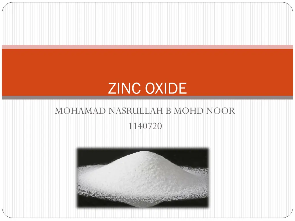
Introduction Zinc oxide ( ZnO ) is a two until twelve compound semiconductor having wide band gap 3.3 eV. It has large exciton binding energy of 60meV at room temperature. It is nontoxic material which is cheaply available ZnO is a material of huge technological importance. It has applications in optoelectronic devices such as solar cell, optical wave guide, light emitting diode and transparent thin films. Thin films of zinc oxide can be prepared by various techniques: 1. Sputtering. 2. chemical vapour deposition ( CVD ). 3. Laser ablation. 4. Sol-gel process. 5. spray pyrolysis.
Fabrication and Characterization of Fabrication and Characterization of Macroporous Oxide Oxide Macroporous Zinc Zinc the fabrication of porous zinc oxide ( ZnO ) via electrochemical etching The samples were characterized by means of scanning electron microscopy ( SEM ) and photoluminescence ( PL ) spectroscopy. For the SEM result,macropous ZnO with highly symmetry hexagonal pits were successfully obtained while for the PL result show the enhancement of near band edge emission for the etched sample. scientific research have been more focused in the areas of porous and nanostructured media. This is due to the potential applications such as light emitting devices,sensors and solar cells highest increase of the surface to volume ratio in the nanostructure and porous ZnO also can enhance in ZnO based on device performance.
There are two method,1-D growth method and electrochemical etching This method will lead to high reproducibility as compared to others The surface information of unetched and etched samples were accessed using FESEM AND PL.
Thickness dependent growth of low temperature atomic Thickness dependent growth of low temperature atomic layer deposited zinc oxide film layer deposited zinc oxide film ZnO properties represent challenge to obtain homogenous thin films that satisfy specific application. From the result ,polycrystalline structure of the wurtzite is the main phase of the ALD sample with OH groups on their surface crystalline ZnO thin films within a broad range of thickness and roughness can be obtained for optic or optoelectronic application These method only used for first layer because solution itself can damage former deposite material effect of ALD deposition temperature and number of cycles,thickness and roughness of film observed by SEM for confirmation through analysis and fitting of the ellipsometric spectra thickness dependent on the number of cycles for ALD growth
Zinc oxide Zinc oxide- -chitosan chitosan nanobiocomposite nanobiocomposite for urea sensor for urea sensor To immobilize ureas and glutamate dehydrogenase for urea detection,zinc oxide-chitosan nanobiocomposite film onto indium-tin-oxide coated glass has been used. presence of ZnO nanoparticles in Chitosan results and enhanced electron transfer kinetics. Most urea biosensors based on urease Urs are based on catalytic conversion of urea to hydrogen bicarbonate and ammonium Thus, glutamate dehydrogenase ,GLDH has been used as an alternate since it catalyzes the reaction. Zinc oxide (ZnO) nanoparticles have been used for fabrication of transducer surface because of their unique ability to promote faster electron transfer between electrode and active site of desired enzyme. Efforts should be made to utilize this bioelectrode for estimation of urea in serum samples and utilize it for fabrication of other biosensors.
Formation of zinc oxide films using submicron zinc particle Formation of zinc oxide films using submicron zinc particle dispersions dispersions The thermal oxidation as a method of submicron metallic Zn particles to form nanostructured ZnO films. The characterized of this particles are surface morphology and oxidation characteristics. Due to differential thermal expansion between metallic Zn core and Zn shell , nanoflakes , nanoribbons , nanoneedles , and nanorods were formed . To produce films at lower costs,efforts have focused on solution-based methods including sol-gel and oxide nanoparticles dispersions. Another approach ,to form stable molecular precursors at low temperature.The large grain ZnO films were formed after post annealing the printed film or spin-coated The results on the thermal oxidation of films formed by spin coated submicron zinc particles were characterized using TGA,TEM,HIM and XRD
An anode with An anode with aluminium organic light emitting device organic light emitting device aluminium doped zinc oxide thin film for doped zinc oxide thin film for Doped ZnO are attractive alternative materialas transparent conducting electrode because they are nontoxic and inexpensive compare to ITO Organic light emitting diodes(OLEDs) based on organic small molecule and polymer have been studied for potential application especially in the field of flat-panel display. in conventional OLEDs,cathode must minimize while anode must maximize improvement to electrical conductivity of AZO film grown by CVD and PLD device performance of OLEDs was measured for current efficiency 2.9 cd/A and for current density 100 mA/cm compareable to ITO.
Temperature dependent optical properties of Temperature dependent optical properties of pentacene film on zinc oxide film on zinc oxide pentacene The optical transitions of pentacene films deposited on ZnO have been studied by absorption spectroscopy The two Davydov components of the excitions for different film thicknesses has been observed dependence a unique temperature The feasibility of this concept has been demonstrated for the case of p-n junction diode comprising layers of the p-type organic semiconductor pentace deposited onto n-type ZnO substrates. To determine the electronic transitions in pentacene films,its must use optical absorption spectroscopy and almost no thickness dependence at room temperature(RT).
DEVICE Most screen are made of numerous tiny dots or pixels,each emitting its own color. These pixels are powered by thin film transistor technology,and they are typically made using silicon. silicon or gallium arsenide are high cost,toxicity,low stability and poor optoelectronic properties compare to indium gallium zinc oxide ( IGZO ). more suitable and stable for the better performance and battery life low off current,means that less energy goes towards powering display IGZO can unlock higher pixel density,giving higher display resolution. IGZO also related with etching and annealing for developing this device previous method measuring this etch rate inconsistent result. Thus with new materials,new method of analysis
One of the most exciting things is that started using quartz crystal monitor measurements or QCM The optical, semiconductor, solar cell, and thin film display (OLED) industries, to name a few, use quartz crystal monitoring in their production processes