BJT Capacitances in Integrated Circuits
Vertical NPN and substrate PNP transistors are crucial components in integrated circuits. Learn about their structures, characteristics, and small-signal models. Explore BJT output characteristics and capacitances in forward active regions.

Download Presentation

Please find below an Image/Link to download the presentation.
The content on the website is provided AS IS for your information and personal use only. It may not be sold, licensed, or shared on other websites without obtaining consent from the author. If you encounter any issues during the download, it is possible that the publisher has removed the file from their server.
You are allowed to download the files provided on this website for personal or commercial use, subject to the condition that they are used lawfully. All files are the property of their respective owners.
The content on the website is provided AS IS for your information and personal use only. It may not be sold, licensed, or shared on other websites without obtaining consent from the author.
E N D
Presentation Transcript
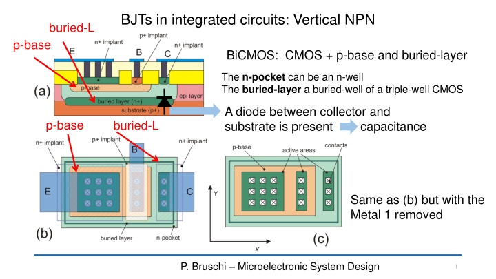
BJTs in integrated circuits: Vertical NPN buried-L p-base BiCMOS: CMOS + p-base and buried-layer The n-pocket can be an n-well The buried-layer a buried-well of a triple-well CMOS A diode between collector and substrate is present capacitance p-base buried-L Same as (b) but with the Metal 1 removed P. Bruschi Microelectronic System Design 1
The lateral PNP Slower than vertical devices due to large base series resistance (rbb') and base-to substrate capacitance Lower early voltage (VA), due to non-optimal collector doping. Larger than vertical devices for the same current capability P. Bruschi Microelectronic System Design 2
The substrate PNP: compatible with standard CMOS n-well processes Limitation: The collector is committed to the substrate, (forced to VSS) P. Bruschi Microelectronic System Design 3
BJT output characteristics Forward Active Region Saturation 0.2 V CESAT V VBE, VCE: control voltages IC, IB: dependent currents P. Bruschi Microelectronic System Design 4
BJT model in the forward active zone V V BE = + V 1 CB I I e T C S V = V V V A CB CE BE I = C I B F Sometimes this expression is used in order to refer to VBEand VCEas control voltages: V V V BE V + CE 1 I I e T C S A For calculation of ICand IBin all operating zones (saturation, cut-off, forward active, reverse active) the Ebers-Moll model should be used. P. Bruschi Microelectronic System Design 5
BJT: small signal model 1 Small signal dc model I V V I = r = C g r A be F m g 0 T m C Equivalence with the MOSFET parameters 1 I 1 g 1 I = = = = D g r m d V I TE d D D BJT V MOSFET V T TE 1 V A P. Bruschi Microelectronic System Design 6
BJT capacitances in forward active region (vertical npn) C = JC c bc m + 1 jc V CB V JC C = JS c cs m + 1 js V CS V JS Transition frequency C = + = JE c C c g 1 be de m de F m f je V V 1 BE T 2 F JE P. Bruschi Microelectronic System Design 7
BJTs in Integrated Circuit: instance parameters area area minimum size BJT ("elemental" BJT) area=1.5 area may not be an integer (not all PDKs allow this) parameter "area" (dimensionless) area=2 (,3, 4 .) area = integer P. Bruschi Microelectronic System Design 8
BJT sizing: Effect of the area parameter on the electrical parameters Electrical effects of area parameter: elemental BJT with area specified as an instance parameter elemental BJT IS VA CJE .. area IS VA area CJE .. P. Bruschi Microelectronic System Design 9
BJT sizing: Gummel plot and beta plot My BJT has to carry this current (200 mA). The elemental BJT would be damaged Using a BJT with area=100 would be equivalent to make the elemental BJT work with a current 100 times smaller. This corresponds to the operating point given by the blue line This refers to the elemental BJT (area=1) IC VBE Gummel Plot Beta Plot P. Bruschi Microelectronic System Design 10


")