Learn about designing a CMOS differential amplifier with current mirror load for achieving high Common Mode Rejection Ratio (CMRR) and high gain, suitable for low supply voltages. The design involves differential to single-ended conversion and maximizing CMRR and gain for optimal performance.
Please find below an Image/Link to download the presentation.
The content on the website is provided AS IS for your information and personal use only. It may not be sold, licensed, or shared on other websites without obtaining consent from the author. If you encounter any issues during the download, it is possible that the publisher has removed the file from their server.
You are allowed to download the files provided on this website for personal or commercial use, subject to the condition that they are used lawfully. All files are the property of their respective owners.
The content on the website is provided AS IS for your information and personal use only. It may not be sold, licensed, or shared on other websites without obtaining consent from the author.
E N D
Presentation Transcript
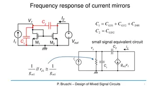
CMOS differential amplifier with current mirror load High CMRR: we start from here: Differential to S/E conversion High CMRR (> 80 dB) High gain (~ 40 dB) at low supply voltages (Vdd-Vss). - = . . i i m id g v v R (for D M 1 2 d d = = . . ic i i C M 1 2 d d os ( ) = - = ) v R i i R R 2 1 1 2 od D d d D D The low Ac shown for the fully-differential case is due Small value of Id common mode variations The output voltage is proportional to id1-id2 P. Bruschi Microelectronic System Design 1
Operating point : Vid=0 = = V V V 1 2 i i C Symmetrical stimulus, but . The circuit is not symmetrical = 2exactly? I I 1 D D ( ) = , , I f V V V D GS BS DS P. Bruschi Microelectronic System Design 3
Demonstration of the exact symmetry of the electrical solution for Vid=0 M1 and M2 0 V V V V V V = = = = 1 2 iD GS V GS V 1 2 1 2 S S V BS BS = 2? = = I I I I 1 DS DS 3 1 D D M3 and M4 4 2 D D = = = V V V V V V 3 4 GS GS 3 4 4? BS BS 3 DS DS P. Bruschi Microelectronic System Design 4
+ = + V V V V 1 3 2 4 DS DS DS DS Proof by contradiction (reductio ad absurdum) = = I I I I 3 1 D D > I I 1 2 D D 4 2 D D > V V 1 2 DS DS > I I 3 4 D D > V V 3 4 DS DS + > + V V V V Contradiction 1 3 2 4 DS DS DS DS P. Bruschi Microelectronic System Design 5
Solution valid everytime Vd=0 = = I I I I 3 1 D D 4 2 D D K = V V 1 2 DS DS = V V 3 4 DS DS = V V out K P. Bruschi Microelectronic System Design 6
Differential mode gain The gain is of the order of???? Independently from the supply voltage ( ) = / / = / / A g r r R r r 2 1 2 4 2 4 d m d d out d d 1 + 1 I 1 = A g = r = A g 1 d m d l I l I l 1 1 1 d m 2 2 4 4 D D D + r r 2 4 d d = = I I I 1 + g I 2 4 1 D D D = 1 m A d l l 1 2 4 D P. Bruschi Microelectronic System Design 9
Differential mode gain In order to obtain a large differential- mode gain it is necessary to: Set VTEto a small value Use long mosfets (small ) 1 + g I = 1 m A d l l 1 2 4 D 1 g I @ m V D TE In strong inversion. Minimum VTE=50 mV - V V GS t = V 2 1 1 + TE In weak inversion. VTE 35-40 mV = A mV d V l l T 1 2 4 TE P. Bruschi Microelectronic System Design 10
Common mode gain = = = / / R r r 2 4 out d d v i occ i R i out out i - for dv = 0 1 2 occ d d v R = = c i i 1 2 d d 2 vc vc os = 0 occ i 0 0 v A CMRR = = = out c Is it possible?? P. Bruschi Microelectronic System Design 11
Common mode gain The problem occurs when we calculate iocc. Placing a short circuit across the output port, disrupts the symmetry: 1 0 ds ds v v g 0 i = = - 4 3 1 d 3 m vc vc 1 v i v v v v = - - = - 1 1 1 2 1 1 ds d s ds s ds g 3 m i i i i 1 2 d d 0 occ i i i = - 4 2 d d 3 4 d d P. Bruschi Microelectronic System Design 12
Common mode gain It is possible to exactly calculate iocc, taking into accout the actual id1/id2ratio and id4/id3ratio . vk but this is a very tedious approach There is a much simpler way: Let us remove the short circuit and directly calculate vout. Now , for vid=0, the circuit is symmetric again and, in particular: vk=vout 1 out k d m g vc vc v = = - @- c v v i 1 2 R g 3 3 os m P. Bruschi Microelectronic System Design 13
Common mode gain 1 v = = - out v A C 2 g R 3 c m os = 0 v d vk for Ros=rd (worst case) A A 2 ( ) ( ) 2 / / d CMRR g R g r r g r = = vc vc 3 1 2 4 m os m d d m d c A CMRR of 80 dB can be easily reached P. Bruschi Microelectronic System Design 14
Large-signal dc transfer function V V = + = - V V V V D D 1 2 i C i C 2 2 ( ) D V ( ) 0 = (0) = - V V V V V 3 out out k DD GS = + - V V V V 3 GS tp GS tp 3 2 D I b In strong inversion 3 3 P. Bruschi Microelectronic System Design 15
Large-signal dc transfer function Vout variations for small VD variations around the origin D = D V R I gm1 out out OCC dI dV D = D occ I V OCC D D = 0 V D P. Bruschi Microelectronic System Design 16
Large-signal dc transfer function ) DQ OCC V I D ( D = V R out out dI dV D = D occ I V OCC D D = V V D DQ dI dV ( ) D = D occ V V R V out D out DQ D = V V D DQ P. Bruschi Microelectronic System Design 18
Approximate dc transfer characteristic -VDMAX VDMAX - V V DD SS V D D A d Example: Ad=100, Vdd-Vss=5V VD<50 mV P. Bruschi Microelectronic System Design 19
Practically constant and equal to gm1 dI dV ( ) D = D occ V V R V out D out DQ - V DASAT V D = V V 4 dd D DQ = / / R r r 2 4 out d d M4 enters triode region and rd4 drops down M2 enters triode region and rd2 drops down P. Bruschi Microelectronic System Design 20
Minimum output voltage V DSAT V 2 2 DS ( ) V V V V V V DSAT V = - = - - 2 2 2 2 2 DS out S out i GS V V V DSAT V - + 2 2 2 out i GS V VD in the linear zone is at most a few tens mV VC varies between VSS and VDD V - D C 2 V V V DSAT V - + 2 2 out C GS P. Bruschi Microelectronic System Design 21
Minimum output voltage ( ) min = - + V V V DSAT V 2 2 out C GS Weak inversion Strong inversion 100 mV @ V DSAT V V 2 @ = - DSAT V V V 2 2 GS tn 2 GS tn ) ( ) min = - V V V ( min = - + 100 mV V V V out C tn out C tn P. Bruschi Microelectronic System Design 22
Minimum Vdd-Vss = + + V V V V 1 3 dd outS DS DS |VDS3| = V V 3 3 DS GS VDS1 ( ) min = + + V V DSAT V V 1 3 dd MIN GS Example: VMIN=100 mV VDSAT2=100 mV |VGS3|=0.5 V VoutS min( ) @ 0.7 V V dd P. Bruschi Microelectronic System Design 24
Input common mode range Lower limit As VCis progressively decreased, also VS decreases at the same pace and eventually the voltage across the current source I0will get smaller than the minimum value VMIN. From that point on, I0will rapidly decrease, turning off the stage. V V C C ( ) C V min = + + V V V 1 SS MIN GS P. Bruschi Microelectronic System Design 25
Input common mode range Upper limit As VCis progressively increased, also VS increases at the same pace. Since Vout=VK=VD2 = VD1is fixed, eventually VDS1and VDS2will drop below the saturation voltage. V V V V = - ( 3 dd GS C GS V V V V - - - vk 1 1 1 ) DS K S DSAT V DSAT V V 1 1 C C V V V DSAT V V - + - 3 1 1 dd GS GS C P. Bruschi Microelectronic System Design 26
Input common mode range V V V DSAT V V - + - 3 1 1 dd GS GS C = + - V V V V 3 3 3 3 GS tp GS tp ) 1 ( = + - V V V V 1 1 1 GS tn GS tn ( ) C V ( ) max = - + - - + - - V V V V V V V DSAT V 3 1 3 3 1 1 1 dd tp tn GS tp GS tn The input common mode voltage can get even slightly higher than Vdd P. Bruschi Microelectronic System Design 27