Digital Logic Design: Sequential Circuits & Latches
Explore the world of digital logic design with a focus on sequential circuits, latches, and storage elements. Learn about level-sensitive devices, edge-triggered flip-flops, SR latches, and cross-coupled inverters. Understand the operation and characteristics of these essential components in building large systems. Discover how clock signals synchronize circuit states and enable reliable data storage in binary storage devices.

Uploaded on Mar 16, 2025 | 6 Views
Download Presentation

Please find below an Image/Link to download the presentation.
The content on the website is provided AS IS for your information and personal use only. It may not be sold, licensed, or shared on other websites without obtaining consent from the author.If you encounter any issues during the download, it is possible that the publisher has removed the file from their server.
You are allowed to download the files provided on this website for personal or commercial use, subject to the condition that they are used lawfully. All files are the property of their respective owners.
The content on the website is provided AS IS for your information and personal use only. It may not be sold, licensed, or shared on other websites without obtaining consent from the author.
E N D
Presentation Transcript
COE211: Digital Logic Design Synchronous Sequential Logic
COE211: Digital Logic Design Sequential Circuits: Latches
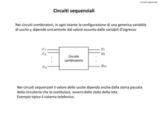
Sequential Circuits Outputs Inputs Combinational circuit Flip Flops Next state Present state Timing signal (clock) Clock a periodic external event (input) Clock synchronizes when current state changes happen keeps system well-behaved makes it easier to design and build large systems 3 / 14
Storage Elements Binary storage device capable of storing one bit Latch = level-sensitive device Control signal: Enable State changes with input when enabled (e.g., when Enable = 1) Holds last input value when disabled (when Enable = 0) Flip-flop = edge-triggered device Control signal: periodic Clock State of flip-flop can only change during clock transition Example: Flip-flops change on rising/falling edge of clock Why change on an edge? Couldn t we change state while clock is 1? That would be a latch! Edge is moment in time, state is duration conditions 3/16/2025 COE211: Digital Logic Design 4
Level-sensitive vs Edge-triggered Latches are level-sensitive Flip-flops are edge-sensitive 3/16/2025 COE211: Digital Logic Design 5
Latchs Characteristics Can store one bit of binary information Level-sensitive devices, asynchronous SR Latch Named after functionality: S = set, R = reset Specification: Inputs: S and R Outputs: Q and Q SR Latch Operation: Q=1 and Q =0 when in set state Q=0 and Q =1 when in reset state Inputs should be 0 unless pulse on S or R sets or resets latch 3/16/2025 COE211: Digital Logic Design 6
Cross-coupled Inverters A stable value can be stored at inverter outputs 0 1 1 0 State 1 State 2
SR Latch Set and Reset are stable states If S=0 and R=0, then state will not change by itself 3/16/2025 COE211: Digital Logic Design 8
SR Latch with NORs SR latch is made from two cross-coupled NORs Usually S=0 and R=0 When Q = 1, the SR -Latch is in the Set state When Q = 0, the SR -Latch is in the Reset state S=1 and R=1 generates illogical results R S Q Q R (reset) Q 0 1 1 0 Stable 0 0 1 0 Set 0 1 Reset 0 0 Undefined 0 1 1 0 1 1 Q S (set)
SR Latch with NANDs SR latch is made from two cross-coupled NANDs Sometimes called RS latch Usually S=1 and R=1
SR Latch with control input Avoid uncontrolled latch changes C = 0 disables all latch state changes Control signal enables data change when C = 1
D Latch Q0 indicates the previous state (the previously stored value) X S D Q C Q R Y X Y C Q Q 0 0 1 Q0 Q0 Store 0 1 1 0 1 Reset 1 0 1 1 0 Set 1 1 1 1 1 Disallowed X X 0 Q0 Q0 Store D CQ Q 0 1 0 1 1 1 1 0 X 0 Q0 Q0
D Latch Input value D is passed to output Q when C is high Input value D is ignored when C is low X S D Q C Q R Y D C Q Q 0 1 0 1 1 1 1 0 X 0 Q0 Q0
D Latch Z only changes when E is high If E is high, Z follows X x D Q z C E If C = 0, the D latch stores data indefinitely regardless of input D values Forms basic storage element in computers
Symbols for Latches SR latch, based on NOR gates S R latch, based on NAND gates D latch can be based on either NOR or NAND D latch, sometimes called transparent latch
Summary Latches are based on combinational gates (e.g. NAND, NOR) Latches store data even after data input has been removed RS latches operate like cross-coupled inverters with control inputs (S = Set, R = Reset) With additional gates, a RS latch can be converted to a D latch (D stands for Data) D latch operation is simple When C = 1, data input D stored in latch and Q = D When C = 0, data input D is ignored and Q = previous latch value
D Latch - Summary 3/16/2025 COE211: Digital Logic Design 19
Edge-triggered D Flip-Flop Construct D flip-flop from two latches: Primary latch: Reads value of D while CLK is high Is disabled when clock is low Secondary latch: Is disabled when CLK is high (i.e., holds previous value) Takes value from master on negative edge of clock 3/16/2025 COE211: Digital Logic Design 20
Positive and Negative Edge D Flip-Flops There exist positive and negative edge trigger D FF Bubbled Clock (C) means negative edge trigger We may need other FFs to synchronously set or reset the FF state and/or complement the previous state Lo-Hi edge Hi-Lo edge
Positive Edge-Triggered J-K Flip-Flop Created from D FF K resets J sets J=K=1 inverts Q J K CLK Q Q 0 0 0 1 1 0 1 1 Q0 Q0 0 1 1 0 Q0 Q0
Clocked J-K Flip Flop J: set, K: reset, if J=K=1 then toggle output Characteristic Table
Positive Edge-Triggered T Flip-Flop Created from JK or D F.F. T CLK Q Q T=0 No change 0 1 Q0 Q0 Q0 Q0 T=1 invert Q
Characteristic Table and Equation J D T Q Q Q Q Q Q K J 0 0 1 1 K Q(t+1) 0 Q(t) 1 0 1 Q (t) D Q(t+1) T Q(t+1) 0 0 0 Q(t) 0 1 1 1 1 Q (t) Q(t+1) = D Q(t+1) = JQ (t) + K Q(t) Q(t + 1) =TQ + T Q
Asynchronous Inputs J, K are synchronous inputs Effects on the output are synchronized with the CLK input Asynchronous inputs operate independently of the clock and synchronous inputs Set/reset the FF to 1/0 states at any time
Asynchronous Inputs Reset signal (R) is active low R = 0 clears the output Q This event can occur at any time, regardless of the value of the CLK
Parallel Data Transfer Flip flops store outputs from combinational logic Multiple flops can store a collection of data
Summary Flip flops are powerful storage elements They can be constructed from gates and latches! D flip flop is simplest and most widely used Asynchronous inputs allow for clearing and presetting the flip flop output Multiple flip flops allow for data storage The basis of computer memory! Combine storage and logic to make a computation circuit