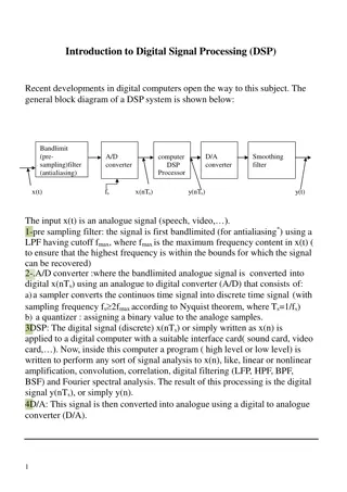
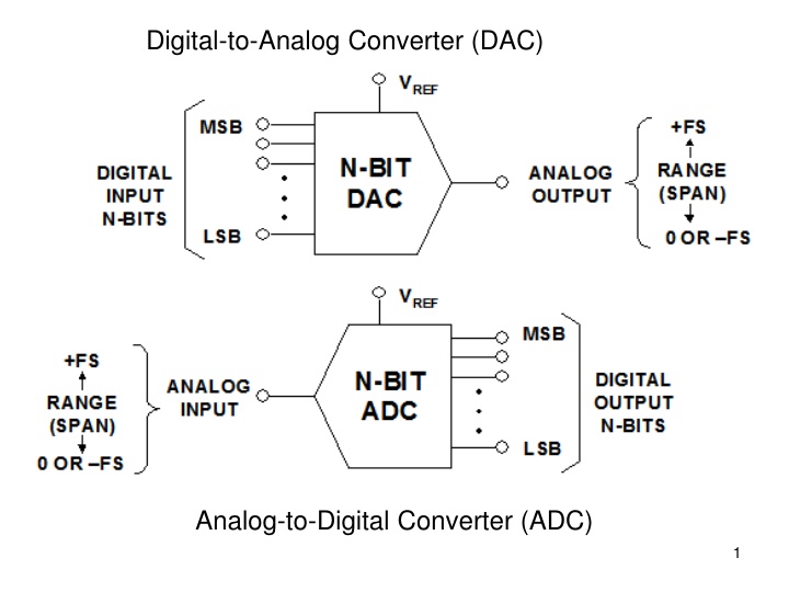
Fundamentals of Digital-to-Analog Converter (DAC) and Analog-to-Digital Converter (ADC). Learn about transfer curves, ideal DAC/ADC behavior, binary codes, and modeling techniques. Understand the concept of VREF and VLSB, and discover the significance of offset binary codes in 3-bit DAC/ADC systems. Ideal transfer curves of high-resolution converters are also discussed.
Please find below an Image/Link to download the presentation.
The content on the website is provided AS IS for your information and personal use only. It may not be sold, licensed, or shared on other websites without obtaining consent from the author. If you encounter any issues during the download, it is possible that the publisher has removed the file from their server.
You are allowed to download the files provided on this website for personal or commercial use, subject to the condition that they are used lawfully. All files are the property of their respective owners.
The content on the website is provided AS IS for your information and personal use only. It may not be sold, licensed, or shared on other websites without obtaining consent from the author.
Ideal DAC Digital input code: straight binary Analog output voltage: unipolar V V = = = ( ) * * * FSR N V D D V D D REF N o in in LSB in in 2 2 1 Digital input code: offset binary Analog output voltage: bipolar: V V D D = 2 REFN V V + = + ( ) * * REFP FSR N REFN V D REFN V o in in in N 2 1 4
Ideal ADC Digital output code: 0, 0 if V in V V = ( ) ( ), in D V round else out in LSB = N 2 1, if V V V V in REF LSB FSR 0, if V REFN V in V REFN V = ( ) ( ), in D V round else out in V LSB N 2 1, if V REFP V V in LSB 8
HW: DAC modeling Every student group will create a Matlab model of a DAC To be shared with all students Talk among all, but select your own architecture For static models, Vo=Vo(Din) Model consists of a vector of Vo s, indexed with the DAC input code Din. 11
HW: DAC modeling For dynamic models, include only the previous code dependence For each code transition, the output is not a single value, but a waveform made of a select number of samples For the first value in Din, just get the static Vo Beginning from the second values in Din, the waveform depends on both the previous code and the current code 15
HW: DAC modeling For each of these transitions, we can model it with a 1st or 2nd order step response of an RC circuit The R and C values corresponding to each Din can be computed with the static model The RC parameterized step responses are used to interpolate between the static Vo to create the dynamic waveform Details will be discussed for each DAC 16
The Kelvin Divider (String DAC) V7 3-bit string DAC: Vref and gnd 8 unit resistors 8 tap voltages 3 digital input 3 to 1 of 8 dec analog Vout Vout buffer V6 V5 V4 V3 + V2 V1 V0 N-bit version consists of 2N equal resistors in series and 2N switches Need N-bit binary to 1 of 2N decoder If input code = k, analog output the kth tap voltage. 17
Model in Matlab Vref can also be normalized to 1 Unipolar V range: 0 to 1 Alternatively can have two resistors of R/2 at Vref and gnd, shift tap voltages by 0.5 VLSB Bipolar V range: -1 to 1 Resistor can also be normalized to have nominal value of 1 Rk = Rnom*(1+ k) k randomly generated Make sure Rk >= Rmin. 18
The standard deviation of k depends on both the process and the area Explore how this standard deviation is related to the errors in the transfer curve For a given DAC, once fabricated, The Rk values are fixed The tap voltages are fixed The static transfer curve is fixed an array containing Vk at k-th entry 19
A simple linear RC model From k1 to k2: Use target code k2 for RC value Ro ~= k2*RN // (2^N k2)*RN + Ron Co ~ constant if transmission gates used Initial value is Vk1, on Co Final value is Vk2, on Co 1st order RC settling closed form solution of waveform 21
If trimming points are included: After fabrication trimming to make the 3 major nodes to be at approximately the correct voltages Model as a single string but 4 voltage dividers 22
Thermometer current DACs Output node at virtual ground Each resistor contributes either 0 or Vref/R If input digital code = k, k of the 2N 1 switches will be turned on I_out =I1 + I2 + +Ik k*Vref/R Inherently monotonic 23
Use Matched Current Sources Current mirrors to create identical current sources CMOS current sources are compact Cascode current mirrors to increase output impedence I_out =I1 + I2 + +Ik k*I Inherently monotonic 24
Use Complementary outputs Each current source and the two switches form a differential pair Differential pair input Vinh and vinl are just enough to steer all tail current clearly to left or right All tail currents in current mirror connection The on side diff pair transistor and tail current transistor in cascode Can cascode tail current source, to achieve double cascode R_out 25
HW for everyone Generalize the previous page to an N-bit structure Assume all resistors have ideal values as you specify Let MSB be controlled by b1, , and LSB be controlled by bN Show that Vout = sum{ bi * Vref/2^i} for i=1 to N 27
4-Bit R-2R Ladder Network One of the most common DAC building-block structures Uses resistors of only two different values with ratio 2:1 An N-bit DAC requires 2N resistors, easily trimmable two ways in which the R-2R ladder network may be used as a DAC 29
Voltage-Mode R-2R Ladder "rungs" or arms of the ladder are switched between VREF and ground Output node has output impedance = R, may need to buffer 30
HW for everyone Generalize the previous page to an N-bit structure Let MSB be controlled by b1, , and LSB be controlled by bN Show that Vout = sum{ bi * Vref/2^i} for i=1 to N 31
Current-Mode R-2R Ladder Vref/R Series R can be used to adjust gain of DAC R_out is code dependent, leading to DAC nonlinearity 32
HW for everyone Generalize the previous page to an N-bit structure Take the resistor at Vref to be 0 Let MSB be controlled by b1, , and LSB be controlled by bN Show that Iout = Vref/R * sum{ bi /2^i} for i=1 to N 33
Equal Current Sources Switched into an R-2R Ladder Network R R DAC output impedance is constant and equal to R Used in high speed video DAC Low output impedance may be problem Can add unit cell MSBs to form segmented structure Can replace the gnd node by an identical R-2R to form differential structure, which has much better linearity 34
Capacitive Binary-Weighted DAC gnd / Vo C C/2^N C/2 C/2^N gnd Vref The first N caps are controlled by the N bits Last cap is dummy, always connected to gnd 37
HW for one group Create an N-bit segmented CDAC model, with in the 12 to 16 range MSB segment having 6 bits The LSB segment N-6 bits Can have total areas for both segments being equal Compute appropriate C_bridge to make the total effective cap of the LSB seg equal to the unit cap in the MSB array 39
Segmented Voltage-Output DACs LSB MSB MSB LSB Coarse string has 2M equal resistors, must be accurate to M+K bit level Fine stage K-bit DAC must have K-bit accuracy Fine stage could be string DAC or R-2R DAC Use buffers to isolate the two stages, buffers need to be accurate to the M+K bit level 40
HW for one group Model an R DAC, with string coarse DAC and R2R interpolating fine DAC MSB string segment has 5 or 6 bits LSB R2R segment has 6 to 10 bits Include buffer errors: Offset, at 1 mV level random Gain error, at 0.1% level random 41
Unbuffered String DACs Fine string // R 7R/8 Total resistance = 8R, current = Vref/8R Voltage across fine string = Vref/8R * 7R/8 = 7Vref/64 Each resistor in fine string has voltage = Vref/64 42
Segmented Current-Output DACs Instead of turning on and off current, use current steering; Current steering is much faster, suited for high speed Use differential pair as steering switch Use just enough diff voltage to steer the current completely 43
HW for one group Model the thermometer plus R2R current DAC Make the MSB to be 5 or 6 bits Make the LSB to be 6 to 10 bits That is: 5 + {6, 7, 8}; or 6+{8, 9, 10} Add the option of a voltage DAC: I_out ant I_out_bar goes to an I V buffer 44
HW for one group Model a thermometer plus R2R voltage DAC by applying Vref and gnd at Iout and Iout_bar and taking Vout at Vref node Make the MSB to be 5 or 6 bits Make the LSB to be 6 to 10 bits That is: 5 + {6, 7, 8}; or 6+{8, 9, 10} 45
HW for one group Model the multi-segmented current steering DAC as shown on the last page s example use Make the output to be differential with I_out ant I_out_bar Each unit is a PMOS current source with with a differential switch Consider two cases at the output node: I_out ant I_out_bar goes through RL to gnd I_out ant I_out_bar goes to an I V buffer 47
DAC standard test Chapter 6 of book Offset, gain error INL, DNL AC test Settling 48
Offset and Gain Error Both are absolute errors, measured wrt ideal LSB LSBi = ideal range / 2^N Offset in V = Va(C0) Vi(C0) Offset in LSBi = (Va(C0) Vi(C0))/LSBi C0could be 0 0, or first code whose output is not at the lower rail GE = (Va(C1) Va(C0))/LSBi (C1 C0) C1could be 1 1, or last code whose output is not at the upper rail 50


")


")