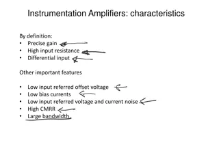
Op-Amp Design Parameters and Calculations Process
Explore the design process and calculation of parameters for an operational amplifier, including offset voltage, aspect ratios, and device specifications. Learn how to optimize performance based on given design requirements.

Download Presentation

Please find below an Image/Link to download the presentation.
The content on the website is provided AS IS for your information and personal use only. It may not be sold, licensed, or shared on other websites without obtaining consent from the author. If you encounter any issues during the download, it is possible that the publisher has removed the file from their server.
You are allowed to download the files provided on this website for personal or commercial use, subject to the condition that they are used lawfully. All files are the property of their respective owners.
The content on the website is provided AS IS for your information and personal use only. It may not be sold, licensed, or shared on other websites without obtaining consent from the author.
E N D
Presentation Transcript
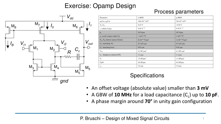
Exercise: Opamp Design Process parameters Parametro n-MOS p-MOS nCox, pCox 240 10-6 A/V2 50 10-6 A/V2 Vtn,Vtp 0.43 V -0.56 V 0.44 V 1/2 0.59 V 1/2 (effetto body) 50 V/ m 50 V/ m k (coeff. termico della Vt) -1 mV / C 1 mV / C 6 10-10 V m2 2 10-10 V m2 Nfn, Nfp (fattore rumore flicker) 8.5 mV m 8.5 mV m CVt (matching Vt) 0.03 m 0.03 m C (matching beta) 6.2 fF/ m2 6.2 fF/ m2 COX 1.2 m 1.2 m LC (lunghezza minima D/S) 1.8 fF/ m2 1.8 fF/ m2 CJ 0.6 fF/ m 0.6 fF/ m Cgdo tox 5.6 nm 5.6 nm Specifications An offset voltage (absolute value) smaller than 3 mV A GBW of 10 MHz for a load capacitance (CL) up to 10 pF. A phase margin around 70 in unity gain configuration P. Bruschi Design of Mixed Signal Circuits 1
Offset specification An offset voltage (absolute value) smaller than 3 mV = = 3 3 mV 1 mV vio vio ( ) ( ) 2 2 A B V V V V = + 2 vio GS t GS t = + = + 2 Vtp 2 2 Vtn A C 1 C B F C 1 C W L W L p n 2 2 1 1 3 3 In order to reduce A and B and then the total area, we choose: = = = = 8.5 mV m C C Vtp Vtn 0.03 m C C p n = 100 mV V V GS t 1 V V V V 1 3 g g GS t = = = 3 m F 1 ( ) 1 m GS t 3 P. Bruschi Design of Mixed Signal Circuits 2
Offset specification = 100 mV V V V V GS t ( ) ( ) 1 = = 300 mV V V V V V V 1 3 g g GS t GS t 3 5 GS t = = = 3 m 1 F ( ) 1 m GS t 3 ( ) ( ) 2 2 V V V V ( ) 2 GS t GS t = + = + 2 Vtp A C 1 C B FC 1 C p Vtn n 2 2 = = 8.5 mV m C C V V V V Vtp Vtn GS t GS t = = 1.5 mV m 1 C 1 C p n = 2.83 mV = m m FC C 2 2 Vtn = 0.03 C A=74.5 10-6V2 m2 B=10.3 10-6V2 m2 p n P. Bruschi Design of Mixed Signal Circuits 3
Offset specification A=74.5 10-6V2 m2 B=10.3 10-6V2 m2 W L W L B A = = = 0.37 3 3 a Optimum area distribution between differential pair and current mirror opt 1 1 opt 1 B = + 2 102 m W L A 1 1 2 vio a opt = 2 38 m W L a W L 3 3 1 1 opt With only the offset specification, we cannot determine other amplifier parameters. Adding the GBW - phase margin specification we can go further into the amplifier design P. Bruschi Design of Mixed Signal Circuits 4
GBW and phase margin A GBW of 10 MHz for a load capacitance (CL) up to 10 pF. A phase margin around 70 in unity gain configuration = = 3 2 0 = , C C C C C + 1 2 c Hypotheses: 2 C C 2 L L = 2 1.88 mS g C GBW 5 m L 1 C C Using the rule of thumb CC=CL: C2 = C g g 1 5 m m L C1 g = 0.63 mS 5 m g 1 m P. Bruschi Design of Mixed Signal Circuits 5
Calculation of device aspect ratios 1.88 mS 0.63 mS g g 5 1 m m W L W L g V ( ) = = = 26.1 5 5 5 m g C V V ( ) 5 m n OX GS t 5 C V 5 5 n OX GS t 5 = 6 2 240 10 A / V C 300 mV n ox g W L = = 126 1 m 1 ( ) C V V 1 p OX GS t 1 100 mV = 50 10 6 2 A / V C p ox W L g V = = 2.92 3 3 = F g = m 0.21 S g ( ) C V 3 1 m m 3 n OX GS t 3 300 mV P. Bruschi Design of Mixed Signal Circuits 6
Determination of M1, M3 and M5 size = 2 102 m W L W L 1 1 1 W L W L = = 114 m W W L L W 1 1 0.9 m 1 1 1 1 1 = 126 1 1 1 1 From offset specs = 2 38 m W L W L 1 3 3 W L W L = = 10.5 m 3 3 W W L L W 3.6 m 3 3 3 1 3 = 2.92 3 3 3 3 From L5=L3 arbitrary constraint = 3.6 m L W L 5 94 m W = 5 26.1 5 5 P. Bruschi Design of Mixed Signal Circuits 7
Determination of M6 and M7 size = I I ( ) 2 6 5 D D = I V V D GS t 2 = ( ) V V V V (Arbitrary constraint) 5 GS t GS t 6 = 6 5 W L W L W L C C W L In order to introduce no penalization in terms of DC gain we can set: L6=L5=3.6 m = = 125 6 5 6 5 C C n OX p OX n OX 6 5 6 5 p OX (Arbitrary constraint) = = 3.6 m L L 7 6 W L = = 450 m 6 W L W L W L W L W L W 6 6 6 5 3 1 2 6 1 2 W L W L L = 6 5 = = 2 28 6 5 7 6 3 W L W L = = 7 3 5 101 m 7 W L 7 3 7 6 7 7 7 3 5 7 P. Bruschi Design of Mixed Signal Circuits 8
Bias and supply currents ( ) V V GS t = = 2 2 2 63 A I I g V g 1 0 1 1 1 1 D m TE m 2 ( ) V V GS t = 282 A 5 I g V g 1 5 5 5 m TE m 2 In order to simplify the design: = = 63 A BI I M8=M7 0 + + Total supply current (including ): 408 A I I I I 0 1 B B P. Bruschi Design of Mixed Signal Circuits 9
Final Design = 2.5 V V dd = = 10 pF C C C L 1 1 = = = 532 R C G g 2 5 m m P. Bruschi Design of Mixed Signal Circuits 10
Check of initial hypothesis validity = = , 10 pF C C C C C C + 1 2 c 2 = = 10 pF C Hypotheses: 2 L L C 10 pF C 2 L = + + C C C C 1 5 2 4 GS DB DB C2 + 2 3 C L W = 1.4 pF C C W L 5 5 5 GS OX C1 = = 0.246 pF 1.67pF C C 2 2 1 DB Jp C 0.023 pF C C L W 4 4 DB Jn C = 2 6.2 fF/ m = C OX = + = ' 1.17 pF C C C C L W C L W = = 2 1.8 fF/ m C C 2 5 6 5 6 DB DB jn C jp C jn jp = 2.16 fF/ m C L The hypotheses are acceptable 1.2 m L , jn p C C P. Bruschi Design of Mixed Signal Circuits 11
Other performance parameters 8 3 1 ( ) + 4.5 10 17 2 2 1 / ( 6.7 nV/ Hz ) S kT F V H Vth z g 1 m 6 10 = 2 10 = 10 2 2 10 2 2 V m V m N N Flicker corner frequency fn fp N W L N k fp fn = + 2 12 2 2 7.42 10 V k F = = at f S VTh S F f F k vF W L 1 1 3 3 k Slew rate: = 165 kHz f F k VTh S I C = = 6.3 V/ s 0 s R c P. Bruschi Design of Mixed Signal Circuits 12
Test-Bench for frequency response RF if, for all frequencies of interest, 1, then: A we can consider that the feedback is not present, thus in terms of small signal: CF Vout Vss (gnd) Vdd VS In DC: Vout=VS. Setting a proper DC value for VSwe can set a correct operating point (e.g. VS=Vdd/2) if R R v F out ( ) A out v A = = d 1 G 1 F R C and A is A F s C D Example: F = 10 1.59 10 Hz f p P. Bruschi Design of Mixed Signal Circuits 13
Amplification from the inverting terminal to the output The open-loop gain that we have found with the testbench of previous slide was not strictly the differential mode gain. That was the gain from the non-inverting input to the output, which is actually a combination of the differential mode and common mode gains. Often, the gain that matters for the stability, is the gain from the inverting input and the output, since in most closed-loop circuits the feedback signal stimulates only the inverting input. In order to simulate this gain, the following circuit can be used: Applies the AC signal (vs) v ( ) out v A A d s Small-signal circuit for f>>fp Sets the DC output voltage P. Bruschi Design of Mixed Signal Circuits 14
Difference between the gains measured from the inverting and non-inverting terminals for the op-amp that we have designed (from simulations) The difference occurs only at frequencies >> f0. Then, to study the stability, we can use one or the other gain, indifferently The difference is due to the different impact of the first-stage singularities (mirror pole, tail pole) Here, the gain obtained from the inverting input is multiplied by -1, (since it is equal to -A) For different designs (different topologies, different specifications, etc.), the differences may be more important. P. Bruschi Design of Mixed Signal Circuits 15