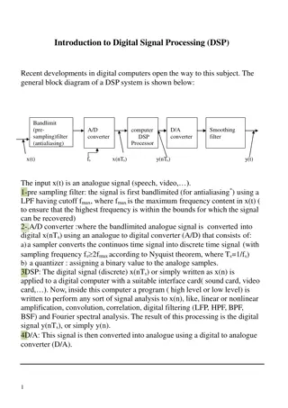
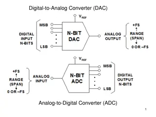
Analog-to-Digital Conversion Techniques
Analog-to-digital conversion can be achieved through different techniques such as voltage-to-frequency conversion, voltage-to-time conversion, and flash (simultaneous) analog-to-digital conversion. Each technique has its advantages and limitations, impacting factors like speed, resolution, and complexity. This process involves converting analog signals into digital form for various applications in electronics and telecommunications.

Download Presentation

Please find below an Image/Link to download the presentation.
The content on the website is provided AS IS for your information and personal use only. It may not be sold, licensed, or shared on other websites without obtaining consent from the author.If you encounter any issues during the download, it is possible that the publisher has removed the file from their server.
You are allowed to download the files provided on this website for personal or commercial use, subject to the condition that they are used lawfully. All files are the property of their respective owners.
The content on the website is provided AS IS for your information and personal use only. It may not be sold, licensed, or shared on other websites without obtaining consent from the author.
E N D
Presentation Transcript
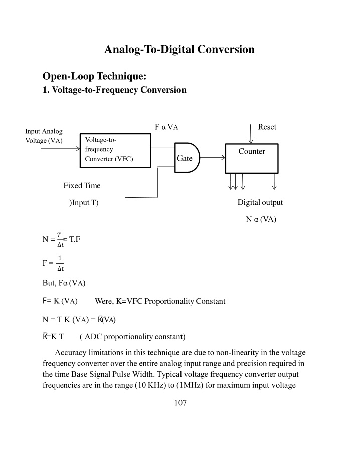
Analog-To-Digital Conversion Open-Loop Technique: 1. Voltage-to-Frequency Conversion F VA Reset Input Analog Voltage (VA) Voltage-to- frequency Converter (VFC) Counter Gate FixedTime Digitaloutput )InputT) N (VA) N = ?=T.F ? 1 F= t But, F (VA) F= K(VA) Were, K=VFC Proportionality Constant N = T K (VA) = K (VA) K = K T ( ADC proportionalityconstant) Accuracy limitations in this technique are due to non-linearity in the voltage frequency converter over the entire analog input range and precision required in the time Base Signal Pulse Width. Typical voltage frequency converter output frequencies are in the range (10 KHz) to (1MHz) for maximum input voltage 107
2. Voltage- To- Time ConversionADC Reset T VA Input Analog Voltage (VA) Voltage-to-time. Converter VTC Gat e Counter Digital output ClockFc N (VA) N= ?= TFC ? 1 Fc= ? But, T (VA) T = K (VA) Where K= VTC ( Proportionality Constant) N= Fc K(VA) = K (V A) K = KFc =ADC Proportionality Constant. 3. Flash (Simultaneous) Analog-to-Digital Converter A comparator is an op. amp. configuration where the voltages of two inputs are compared. If the + input is greater than the - input, the output is a logic high.The flash method utilizes comparators that compare reference voltage with the analog input voltage. When the input voltage exceeds the reference voltage, a HIGH is generated. A comparator is not needed for all 0 s condition. 108
n In general a 2 -1 comparators are required for converting to an n- bit binary code. The number of bits in an ADC is its resolution. Example 1: Design a 2-bit simultaneous A/D converter. Solution: The required number of comparators = 22 1 = 3 where n is the number of bits of the digital output number. Comparators output C2 Low Low High High InputVoltage (V) 0 to +V/4 +V/4 to +V/2 +V/2 + 3V/4 +3V/4 to +V C1 Low High High High C3 Low Low Low High Advantage: Provides a fast conversion times because of a high through put measured in sps (samples per second.) Disadvantage: Large number of comparators necessary for a reasonable sized binary number n no. of comparators = 2 -1 Where n is the number of bits of the output. 109
Example2: Design a 3 bit FlashADC. Solution: 0 0 1 1 1 1 1 110
Example 3: Determine the binary code output of the 3-bit flash ADC for the input with the encoder enable pulses shown in fig. 1. VRef = +8V. Fig.1 Sampling of values on a waveform for conversion to binary code. The resulting digital output sequence: 100 (4), 110(6), 111(7), 110(6), 100 (4), 010(2), 000(0), 001(1), 011 (3), 101 (5), 110 (6), 111(7) Waveform of the resulting digital output sequence: 111
Feedback Techniques 1. Counter Type A/DConverter: A higher resolution A/D converter using only one comparator could be constructed if a variable reference voltage could then be applied to the comparator and when it became equal to the input analog voltage the conversion would be complete. 0 VA Vref This method is much simpler than the simultaneous method for high resolution, but the conversion time required is longer. Since the counter always begins at zero and counts through its normal binary sequence, it may require as many as 2?counts before conversion is complete. The average conversion time is 2? 1counts. 112
Note that the conversion time depends on the size of the input signal 1. Step Size = ??.?/2?-1 2. Number of steps = VA / step size 3. The conversion time = No. of steps * Time 4. The resolution in volt = ??.?/ 2?-1 2. Successive Approximation Analog-to-Digital Converter The Successive-Approximation ADC is one of the most popular types in use today. rate. following Figure shows the basic block diagram of a 4 bit Successive - approximation ADC. It consists of a DAC, Successive-Approximation Register (SAR), and a comparator. 113 It has a relatively simple configuration and an excellent conversion The
The operation diagram for a 3 bit successive - approximation converter ADC is shown below: The time for one analog to digital conversion must depend on both the clocks period (T) and number of bits n. It is given as Tc = n x T Tc: Conversiontime. 114
T: Clockperiod. n: Number of bits. Example 4: An 8-bit successive approximation ADC is driven by 1MHz clock. Find its conversion time. Solution: F=1MHz T=1 ? 1 T= =1 s 1 106 N=8, Tc = n x T 8 x 1 = 8 s Example 5: An 8-bit digital ramp ADC with a 40 mV resolution uses a clock frequency of 2.5 MHz a comparator with VT=1 mV. Determine the following values: 1) The digital output for Vin=6V. 2) The digital output for Vin=6.035V. 3) The max. and average conversion time for thisADC. Solution: The digital output is given by, Count= Vin/ resolution 1) Vin=6 V Count = 6/ 40*10 3 =150
2) count =6.035/40*103 = 150 115 3) (Tc) max= (maximum count)*T =2?-1*1/f =255/25*106 Example 6: A 4 bit digital ramp ADC has an input range of 0 to 7.5 volt. Estimate: Resolution, digital output for an input of 4.25volts and Conversion time if the clock frequency is 1MHz. Solution: Digital output= input/ Resolution in V/LSB Resolution =Vi/ 2?-1 =7.5/16-1=0.5V/LSB D= 4.25/0.5= 8.5LSBs=9 digital output=1001 F=1MHz T=1/f =1/1*106 =1 s N=4bit Tc = 24 x 1 = 16 s
116 4. Integrating Types: A. The Single-Slope Technique: Startpulse Vo(t1) = 1 t1( Vref)dt to RC V (t ) = Vref (t t ) = VA 0 1 1 o ???? RC Vc N = (?1 ??) ?? Slop=Vref/RC Where Fc= ClockFreq. ?1 ?0 ???? Clock
?????=?? ?? ?? ? = ?? ?? (??) =?(??) ?0 ?1 ???? Counter pulse ??? ? = ???????? =??.?? ??? ?0 ???? ?1 117 B. The Dual-Slope TechniqueADC
?1 ?? ( ??)?? = (? ? ) ? 1 1 ? ?(?1)=???? ?? No = 2n 1 = (t1 to) FC ?? ?? (?1 ??) = 118 ?? ?? ?? ? (? ) = ? 1 ?? 1 ? 2 ??(?2) = ??(?1)+ (????)?? = 0 ?1 ?? ?? ?? ???? ? ) = (?2 1 ?? ?? ?? ??? (? ? ) =? 2 1 ?? ?? ?? ???? ? = ? ?? ?? ?? ?
N = N ( VA) N =2n oVref o The Single Slope ADC has a number of disadvantages compared to the Dual-Slope ADC: 1.Convesion time varies with input voltage level, so that specification Noise frequencies are not easily rejected. 2. It depends for its accuracy on a capacitor and a resistor (unstable components). 3. Variations in clock frequency will affect the final recorded output. For these reasons, designers prefer the dual-slope method, although it may be slower than the single slope. The advantages of the dual-slope method are relatively Low cost, simplicity, high accuracy, linearity, and excitant Noise rejection. The one disadvantage of this method is the relatively long Conversion time; it requires 2?+1 clock pulses normally for n bits full scale conversion. 119


 count =6.035/40*10−3 = 150")


")