BJT Current Mirrors & Simple Mirror Design
Explore the design and impact of BJT current mirrors, simple current mirrors, and mirrors with emitter degeneration in microelectronic systems. Understand parameters, base currents, and output resistance for efficient circuit design.

Uploaded on | 1 Views
Download Presentation

Please find below an Image/Link to download the presentation.
The content on the website is provided AS IS for your information and personal use only. It may not be sold, licensed, or shared on other websites without obtaining consent from the author. If you encounter any issues during the download, it is possible that the publisher has removed the file from their server.
You are allowed to download the files provided on this website for personal or commercial use, subject to the condition that they are used lawfully. All files are the property of their respective owners.
The content on the website is provided AS IS for your information and personal use only. It may not be sold, licensed, or shared on other websites without obtaining consent from the author.
E N D
Presentation Transcript
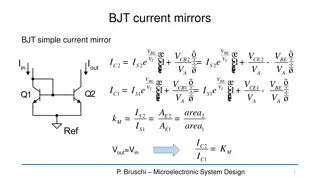
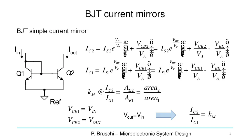
BJT current mirrors BJT simple current mirror V V V V V V BE V BE V = 1 + = 1 + - 2 2 CB V CE V I I e I e BE T T 2 2 2 C S S A A A V V V V V V BE V BE V = 1 + = 1 + - 1 1 CB V CE V I I e I e BE T T 1 1 1 C S S A A A I I A A area area @ = = 2 S k 2 2 E M 1 1 1 S E = = V V V I I 1 CE IN = 2 C k Vout=Vin M OUT V 1 C 2 CE P. Bruschi Microelectronic System Design 1
BJT simple current mirror: parameters V V V Vg = = 1 1 IN CE BE 0.2 V V I V CESAT V = 2 MIN V I = = = R r A A 2 out o 2 C out = = V out out R I V th A P. Bruschi Microelectronic System Design 2
BJT simple mirror: impact of base currents = I I I I I 2 C out = 2 C k M I 1 C i n 1 C I b I b I I I = = 1 2 C C I I = 2 out I C 1 2 B B + + I I 1 2 1 1 2 in C B B I I I = 2@ b b b = 2 out I C 1 I + + I 1 2 C b C b in 1 C 1 + 1 I I I = k = 2 out I C 1 M k 1 b k 1 + M 1 + + M b 1 in C b P. Bruschi Microelectronic System Design 3
BJT simple mirror: impact of base currents 1 + I I I = < out I k k = 2 C k 1 M M k M 1 + M in 1 C b 1 + x@ - 1 for: < < 1 x x 1 + 1 + 1 I k k @ 1 - for: < < 1 out I k M M M b b in + 1 k @ e M R b P. Bruschi Microelectronic System Design 4
Simple mirror with emitter degeneration to increase the output resistance I I I I A A area area = 2 C = = = 2 S k 2 2 E M 1 C 1 1 1 S E V V I R I R = = for Vin=Vout, only if: 1 2 1 1 2 2 BE BE E E E E 1 I I R R I I = + V V R I = = = 1 CE 2 1 E E 1 1 1 IN BE V E + E R I k 1 2 2 E E CE M = V 2 2 2 MIN CESAT E E The voltage drop across RE1 (RE2) makes VINand VMINworse than in the simple mirror I R ( ) @ 1 + @ 1 + 2 V 2 C E R r g R r 2 2 2 2 out o m E o T P. Bruschi Microelectronic System Design 5
BJT current mirror with emitter degeneration: parameters = + V V R I 1 1 1 IN BE E E = + V CESAT V R I 2 2 2 MIN E E I R I R V I ( ) @ 1 + @ 1 + = 1 + 2 V 2 2 V 2 C E C E R r g R r A 2 2 2 2 out o m E o T out T I R Example: with IC2RE2 =225 mV, and VT=25 mV, Rout=10ro2 @ 1 + 2 V 2 C E V V th A T I I I + 1 k = 2 out I C The error due to the base currents is the same as in the simple mirror @ e M + + I I R b 1 1 2 in C B B P. Bruschi Microelectronic System Design 6
The Widlar current source = + V V R I 1 2 2 2 BE BE E E D @ - = @ V V V R I R I 1 2 2 2 2 2 BE BE BE E E E C V V V I I BE V BE V = 1 + @ 2 CB V I I e I e @ ln C V V T T C S S BE T A S I I I I I I I I D @ ln - ln = ln 1 2 1 2 C C C S V V V V BE T T T 1 2 1 2 S S S C R I I I 2 2 E C - I I V @ 2 C e @ R I D @ ln 1 C V V T If Q1=Q2 (IS1=IS2) 2 2 E C BE T 1 C 2 C P. Bruschi Microelectronic System Design 7
The Widlar current source: A non-linear current mirror 2 2 2 T V C I e I current), the behavior is non-linear Since the IC2/IC1ratio is not constant, but depends on IC2(and then on the input R I E C - @ 1 C Slope < d.c gain I I D D I < < out in I = I gain=1 out in out gain<1 The Widlar source was used to produce an almost constant current (Iout) from a variable current Iin > > R I V 2 2 E C T < < R I V @ in I 2 2 E C T P. Bruschi Microelectronic System Design 8
BJT cascode current mirror = + - V V V V 2 1 3 4 CE CE BE BE = V V = V V If we make: I I then: 2 1 CE CE 3 4 BE BE = 2 C k almost independently of Vout M 1 C = V V 3 4 BE BE I I I I = 4 3 C C I I @ ln C V V Design rule 4 3 S S BE T S I I I I I I I I I I I I = = 4 2 S S k = @ 4 4 2 S C C = = 2 S k M M 3 1 S S 3 3 1 S C C 1 S P. Bruschi Microelectronic System Design 9
BJT cascode current mirror: Rout BI 4 ( ) @ 1 + r r h 4 4 v o fe ? be r 4 It can be shown that: There is interaction of the output branch (Q2,Q4) with the input one (Q3,Q4) caused by the base currents. This interaction is not present in the cascode MOSFET h 4 f e @ 41 + R r out o 2 P. Bruschi Microelectronic System Design 10
BJT cascode current mirror: effect of base currents @ = I I I 4 4 2 C E C = = - = - I I I I I I 4 4 4 2 4 out C E B C B I = + + + I I I I I @ BI = 2 C b I 1 1 2 4 in C B B B 4 2 B I - I 2 C b 2 C - + I I I I I I @ = 2 4 out I C B = 1 C b I I I + + I I 1 B + + 2 I 1 2 C b C b 1 1 2 4 in C B B B 1 C 1 b using the approximation: 1 - 1 1 - + y x I I I ( )( ) ( ) @ - 1 1 - = - 1 + + y x x y xy 2 out I C @ 1 b k 1 + + 2 M b 1 in C - 1 + k 1 + I k = - 2 e M 1 2 out I k M @ R M b b in P. Bruschi Microelectronic System Design 11
BJT cascode current mirror: summary of parameters 2 V V V V Vg = + 1 3 IN BE V BE V V CESAT V h = + + 1 4 MIN BE + CESAT g h V I 4 4 fe fe @ 41 + = 1 + R r A out o 2 2 out 1 k = - 2 e M R b The output resistance is increased by a factor around hfe/2, which is paid with an increase of both VINand VMIN. The relative error due to the base current is doubled with respect of the simple mirror. Due to the mentioned drawbacks of the BJT cascode current mirror, other solutions, such as the emitter degenerated mirror and Wilson mirror are often preferred. P. Bruschi Microelectronic System Design 12
Methods to reduce the impact of the base currents: the "beta helper" I = + = + 3 I I I E + I 1 3 1 in C B C 1 b beta helper 3 = + I I I 3 1 2 E B B + 1 + I k I I I = + = + + 1 1 C b M C I I I 1 2 B b B 1 1 in C C + 1 1 b b 3 3 1 + I I = = 2 out I C k 1 b + 1 b M k k + 1 + I I M M in ( ) ( ) 1 1 C C + 1 + 1 b b 3 3 1 b + 1 k e M = - = 2 V Vg R ( ) 2 IN + 1 b b 3 P. Bruschi Microelectronic System Design 13
Simple mirror with emitter degeneration and beta helper This mirror offers a good output resistance and small base-current related error. This made it a popular choice for the design of BJT op-amps. Its large VINprevents its use in low supply voltage circuits ( ) @ 1 + R r g R 2 2 2 out o V m E = 2 + V R I 1 1 IN g E E = + V CESAT V R I 2 2 MIN E E 1 b + 1 k e M = - R ( ) 2 + 1 b b 3 P. Bruschi Microelectronic System Design 14
Mirrors in the 741 Widlar Current source: Bias current Beta helper + Emitter deg: accurate current inverter P. Bruschi Microelectronic System Design 15
Wilson current mirror Target: to obtain the same output resistance of a cascode mirror, but with smaller impact of base currents on the current gain accuracy. Operating principle Note: the Q2-Q1 mirror transmits the output current (Iout) back to the input branch bI 4 inI @ I I 4 E out area area ( ) @ - + 1 I I I b 1 4 out in out @ CI 2 1 ( ) + 1 b area area 4 @ @ I I I 2 out in in area area ( ) + 1 + 1 b 1 1 4 2 P. Bruschi Microelectronic System Design 16
Wilson current mirror: start-up transient = - - I I I I until: 1 4 C p in C B Q2, Q4: off 0 C I = 0 = < < = 2 I V I Vg H 0, = 0, 4 4 2 B C I = I CI Cp in 1 0 I C dV dt Cp = = constant H p As VHapproaches 2V , Q4 and Q2 turn on and the Q2 current is mirrored to M1 P. Bruschi Microelectronic System Design 17
Wilson current mirror IC1starts increasing and taking part of Iin, away from Cp I C dV dt Cp = : decreases H = - - 4:decreases I I I I 1 Cp in C B p Due to the exponential law, small VHincrements produce large IC2(and then IC1) increases Equilibrium is reached when: dV dt 0 0 I H = = Cp = + I I I 1 4 in C B P. Bruschi Microelectronic System Design 18
Wilson Current Mirror: effect of base currents EI 4 = + I I I I 1 4 in C I B I = = - I = + + - I I I I 4 4 4 out C E B 2 1 2 4 C B B B I I area area + + + - I I I I I I I @ @ @ 2 C k 2 = 2 1 2 4 out I C B B B M 1 1 C 1 4 in C B @ I I 2 4 C C 1 1 b 1 b I I b I b 1 + + - + + - I 2 b 2 2 C C C 2 C I I k b I k = 2 C 1 2 4 M = out I 1 2 4 M k b k I 1 + M + I 1 M b C 1 C in 1 C 4 4 P. Bruschi Microelectronic System Design 19
Wilson current mirror 1 1 b 1 b 1 + + - I k b = out I k 1 2 4 M M k b 1 + M in 4 1 1 b 1 b I k b @ 1 + - + - out I k M M k b 1 4 2 4 in M Only if: kM=1 1 b - 1 b 1 b 1 b b 1 b 1 4 b b 2 - = = - 2 b 2 b 2 4 2 4 1 4 1 I ( ) 1 , out I k e e for: k = 1 = + M R R 2 b M in P. Bruschi Microelectronic System Design 20
Wilson current mirror In the Wilson current mirror the relative error due to the base current is of the order of 1/ 2only when it is designed for kM=1. For current gains different from one, the relative error becomes of the order of 1/ . Other characteristics: V V V V = = + @ 2 Vg 2 4 IN H V BE V BE (same as the cascode mirror) = + V 2 4 MIN BE CESAT h due to feedback from Ioutto node H 4 fe @ 41 + R r out o 2 = 2 > = V V V V There is a large systematic error between IC2and IC1 1 2 CE BE CE BE P. Bruschi Microelectronic System Design 21
4-transistor Wilson current mirror The 4-transistor Wilson Mirror is the optimal choice when an accurate mirror with kM=1 is required. = = - = = + = 2 V V V Vg V V V V V V 2 4 1 H BE BE BE CE H g g 2 CE Implementing D1 with a diode- connected BJT (Q3) P. Bruschi Microelectronic System Design 22