HV/HR-CMOS Introduction at Genova - March 12, 2015
Explore the HV/HR-CMOS introduction at Genova with activities including STM chip test, pixel design, and AIDA2020 project details. Follow the progress of this cutting-edge technology development as presented on March 12, 2015, by G. Darbo from INFN/Genova.

Download Presentation

Please find below an Image/Link to download the presentation.
The content on the website is provided AS IS for your information and personal use only. It may not be sold, licensed, or shared on other websites without obtaining consent from the author. If you encounter any issues during the download, it is possible that the publisher has removed the file from their server.
You are allowed to download the files provided on this website for personal or commercial use, subject to the condition that they are used lawfully. All files are the property of their respective owners.
The content on the website is provided AS IS for your information and personal use only. It may not be sold, licensed, or shared on other websites without obtaining consent from the author.
E N D
Presentation Transcript
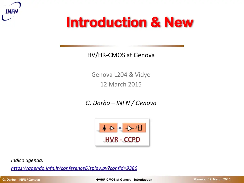
Introduction & New Introduction & New HV/HR-CMOS at Genova Genova L204 & Vidyo 12 March 2015 G. Darbo INFN / Genova Indico agenda: https://agenda.infn.it/conferenceDisplay.py?confId=9386 o Genova, 12 March 2015 HV/HR-CMOS at Genova - Introduction G. Darbo INFN / Genova
STM Chip STM Chip Test chip with 8 pixel (250x50 m2) submitted at STM in December 2014 22 I/O and Power/Ground pads 1 x 2 mm2area The chips will be back on week 26 (June), delayed by 2 months from April date. 2 Genova, 12 March 2015 HV/HR-CMOS at Genova - Introduction G. Darbo INFN / Genova
Pixel Design Pixel Design Design from original Ivan Peric chip N-well detecting element, whole pixel inside n-well, AC coupled, folded cascode 2-stage amplifier with output buffer (maximum load for testing 1pF). Test board in design at Milano. 50 m 250 m 3 Genova, 12 March 2015 HV/HR-CMOS at Genova - Introduction G. Darbo INFN / Genova
STM Chip STM Chip - - Activities Activities Design @ Cadence Cadence software and STM PDK are installed in Genova on a Virtual Linux machine (2 cores, 8GB, 500 + 50 GB) We have the design from Hitesh and Valentino running. Quite well understanding of the design ! Plans for the test We plan to test and compare with simulation the pixels Measure depletion depth with TCT (transient current technique) using the IR laser Measure performance with source and laser We have almost all needed hardware we want to buy some Charge/Voltage amplifier and shaper. In contact with Malte to collaborate and with Gian-Franco to share experience also on 3D sensors 4 Genova, 12 March 2015 HV/HR-CMOS at Genova - Introduction G. Darbo INFN / Genova
AIDA2020 AIDA2020 Project approved on January Funding will come available in June Foreseen a kick-off meting on June 3-5 Our main task in AIDA (as beneficiary) is HV-CMOS hybridization There are other two beneficiaries: Barcelona (Sebastian Grinstein) and Liverpool (Gianluigi Casse) http://aida2020.web.cern.ch 5 Genova, 12 March 2015 HV/HR-CMOS at Genova - Introduction G. Darbo INFN / Genova